

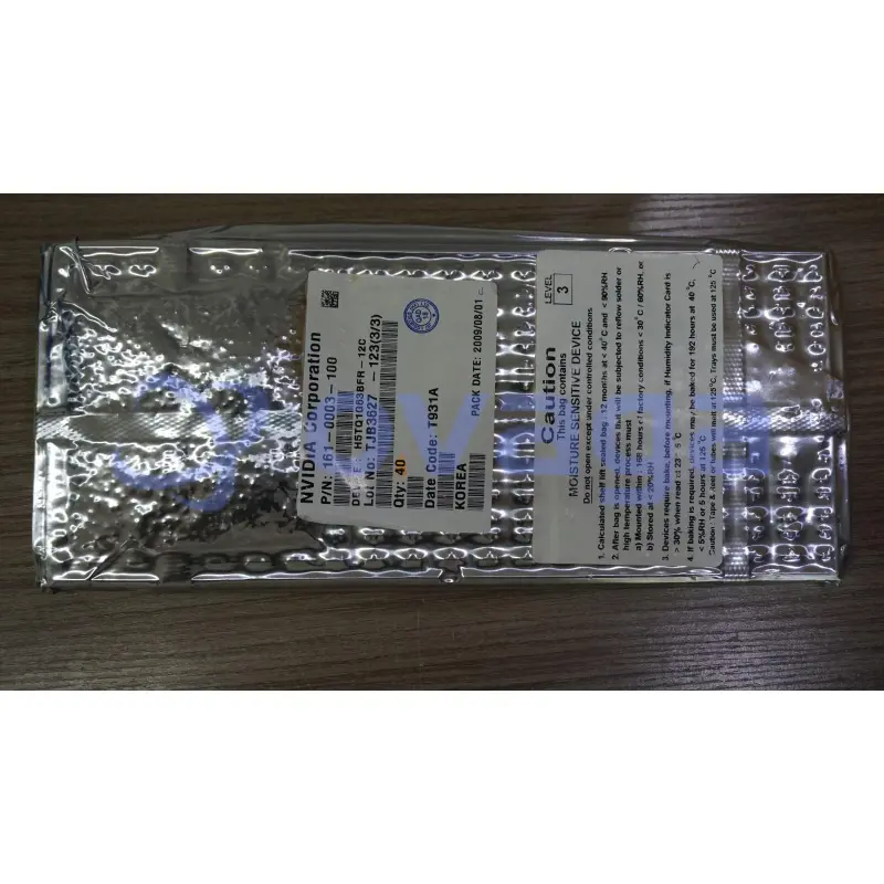
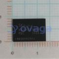
画像は参考用です。製品仕様を参照してください。
注文金額が
$5000H5TQ1G63BFR-12C
High-speed CMOS technology


ブランド: SKHYNIX
製造元部品 #: H5TQ1G63BFR-12C
データシート: H5TQ1G63BFR-12C データシート (PDF)
パッケージ/ケース: BGA-96
製品の種類: メモリ
H5TQ1G63BFR-12C 概要
DescriptionThe H5TQ2G43CFR-xxC, H5TQ2G83CFR-xxC are a 2,147,483,648-bit CMOS Double Data Rate III (DDR3) Synchronous DRAM, ideally suited for the main memory applications which requires large memory density and high bandwidth. SK hynix 2Gb DDR3 SDRAMs offer fully synchronous operations referenced to both rising and falling edges of the clock. While all addresses and control inputs are latched on the rising edges of the CK (falling edges of the CK), Data, Data strobes and Write data masks inputs are sampled on both rising and falling edges of it. The data paths are internally pipelined and 8-bit prefetched to achieve very high bandwidth.FEATURES• VDD=VDDQ=1.5V +/- 0.075V• Fully differential clock inputs (CK, CK) operation• Differential Data Strobe (DQS, DQS)• On chip DLL align DQ, DQS and DQS transition with CK transition• DM masks write data-in at the both rising and falling edges of the data strobe• All addresses and control inputs except data, data strobes and data masks latched on the rising edges of the clock• Programmable CAS latency 5, 6, 7, 8, 9, 10, 11, 12, 13 and 14 supported• Programmable additive latency 0, CL-1, and CL-2 supported• Programmable CAS Write latency (CWL) = 5, 6, 7, 8, 9, 10• Programmable burst length 4/8 with both nibble sequential and interleave mode• BL switch on the fly• 8banks• Average Refresh Cycle (Tcase of0 oC~ 95oC) - 7.8 µs at 0oC ~ 85 oC - 3.9 µs at 85oC ~ 95 oC• JEDEC standard 78ball FBGA(x4/x8)• Driver strength selected by EMRS• Dynamic On Die Termination supported• Asynchronous RESET pin supported• ZQ calibration supported• TDQS (Termination Data Strobe) supported (x8 only)• Write Levelization supported• 8 bit pre-fetch• This product in compliance with the RoHS directive.
特徴
- VDD=VDDQ=1.5V +/- 0.075V
- Fully differential clock inputs (CK, CK) operation
- Differential Data Strobe (DQS, DQS)
- On chip DLL align DQ, DQS and DQS transition with CK
- transition
- DM masks write data-in at the both rising and falling
- edges of the data strobe
- All addresses and control inputs except data,
- data strobes and data masks latched on the
- rising edges of the clock
- Programmable CAS latency 5, 6, 7, 8, 9, 10, 11, 12, 13
- and 14 supported
- Programmable additive latency 0, CL-1, and CL-2
- supported
- Programmable CAS Write latency (CWL) = 5, 6, 7, 8, 9, 10
- Programmable burst length 4/8 with both nibble
- sequential and interleave mode
- BL switch on the fly
- 8banks
- Average Refresh Cycle (Tcase of0 oC~ 95oC)
- - 7.8 µs at 0oC ~ 85 oC
- - 3.9 µs at 85oC ~ 95 oC
- JEDEC standard 78ball FBGA(x4/x8)
- Driver strength selected by EMRS
- Dynamic On Die Termination supported
- Asynchronous RESET pin supported
- ZQ calibration supported
- TDQS (Termination Data Strobe) supported (x8 only)
- Write Levelization supported
- 8 bit pre-fetch
- This product in compliance with the RoHS directive.
応用
- Main memory for mobile devices, such as smartphones and tablets
- Graphics processing units (GPUs) in gaming consoles and high-performance computing systems
- Digital cameras and camcorders for storing images and videos
- Network routers and switches for packet buffering and forwarding
- Embedded systems and Internet of Things (IoT) devices requiring fast and reliable memory access
- Industrial applications for data logging and processing
仕様
| パラメータ | 価値 | パラメータ | 価値 |
|---|---|---|---|
| Product Name | H5TQ1G63BFR-12C | Product Type | Memory |
| Manufacturer | Hynix | Memory Type | DDR3 SDRAM |
| Capacity | 1GB | Interface | Parallel |
| Clock Frequency | 533MHz | Operating Voltage | 1.5V |
| Temperature Range | -40°C ~ 85°C | Mounting Type | Surface Mount |
| Package / Case | FBGA-84 |
配送
| 配送タイプ | 配送料 | リードタイム | |
|---|---|---|---|
 |
DHL | $20.00-$40.00 (0.50 KG) | 2-5 日々 |
 |
フェデックス | $20.00-$40.00 (0.50 KG) | 2-5 日々 |
 |
UPS | $20.00-$40.00 (0.50 KG) | 2-5 日々 |
 |
TNT | $20.00-$40.00 (0.50 KG) | 2-5 日々 |
 |
EMS | $20.00-$40.00 (0.50 KG) | 2-5 日々 |
 |
登録された航空便 | $20.00-$40.00 (0.50 KG) | 2-5 日々 |
処理時間:送料は地域や国によって異なります。
支払い
| 支払条件 | ハンドフィー | |
|---|---|---|
 |
電信送金 | 銀行手数料 US$30.00 を請求します。 |
 |
ペイパル | 4.0%のサービス料がかかります。 |
 |
クレジットカード | 3.5%のサービス料がかかります。 |
 |
ウエスタンユニオン | charge US.00 banking fee. |
 |
送金サービス | 銀行手数料は 0.00 米ドルかかります。 |
保証
1.購入した電子部品には365日保証が含まれており、製品の品質を保証します。
2.受け取った商品の一部が完璧な品質ではない場合、当社は責任を持って返金または交換を手配します。 ただし、商品は元の状態のままでなければなりません。
パッキング
-

ステップ1 :製品
-

ステップ2 :真空包装
-

ステップ3 :静電気防止袋
-

ステップ4 :個包装
-

ステップ5 :梱包箱
-

ステップ6 :バーコード配送タグ


すべての製品は静電気防止袋に梱包されます。 ESD 帯電防止保護を備えた状態で出荷されます。
社外の ESD 梱包ラベルには、部品番号、ブランド、数量などの当社の情報が使用されます。
私たちは出荷前にすべての商品を検査し、すべての製品が良好な状態であることを確認し、部品が新しいオリジナルでデータシートと一致していることを確認します。
すべての商品に問題がないことを確認した後、梱包後、安全に梱包し、グローバルエクスプレスで発送します。 優れた耐穿刺性と耐引裂性を示し、シールの完全性も良好です。


パーツポイント
-
The H5TQ1G63BFR-12C chip is a type of synchronous dynamic random-access memory (SDRAM) used in electronic devices such as smartphones and tablets. It offers a capacity of 1 Gbit and operates at a clock speed of 667 MHz. The chip incorporates multiple memory banks and supports a burst mode for improved data transfer rates. It is commonly used as a main memory in consumer electronics due to its high performance and reliability.
-
Equivalent
The equivalent products of the H5TQ1G63BFR-12C chip are the H5TQ1G63BFR-12C and other related DDR3 SDRAM chips. -
Features
H5TQ1G63BFR-12C is a type of dynamic random-access memory (DRAM) chip with a capacity of 1 gigabit. It operates at a frequency of 800 MHz and has a data transfer rate of 1.6 gigabytes per second. It is designed for use in various electronic devices such as smartphones, tablets, and other mobile devices. -
Pinout
The H5TQ1G63BFR-12C is a memory chip with a pin count of 78. It is a 1Gb LPDDR2 SDRAM chip used in mobile devices and offers high-speed data transfer rates. -
Manufacturer
The manufacturer of the H5TQ1G63BFR-12C is SK Hynix. SK Hynix is a South Korean semiconductor manufacturing company that specializes in the production of memory chips, including DRAM (Dynamic Random Access Memory) and NAND flash. They are known for their high-quality memory solutions, used in various electronic devices such as smartphones, computers, and servers. -
Application Field
The H5TQ1G63BFR-12C is a type of synchronous dynamic random-access memory (SDRAM) chip commonly used in mobile devices such as smartphones and tablets. It provides high-speed data storage and retrieval for applications such as gaming, multimedia playback, and multitasking. -
Package
The H5TQ1G63BFR-12C chip comes in a BGA package type with a form factor of FBGA and a size of 9mm x 11mm.


私たちは高品質の製品、思いやりのあるサービス、販売後の保証を提供します
-

豊富な商品を取り揃えておりますので、お客様の様々なニーズにお応え致します。
-

最小注文数量は1個からとなります。
-

最低国際配送料は0.00ドルから
-

全商品365日品質保証


