

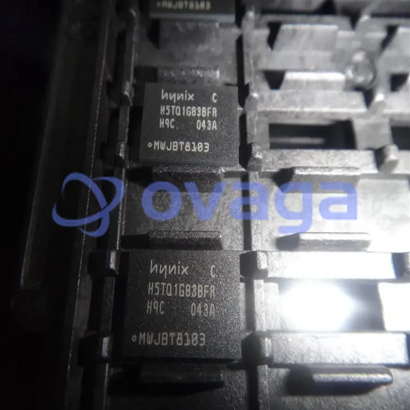
画像は参考用です。製品仕様を参照してください。
注文金額が
$5000H5TQ1G83BFR-H9C
Enables faster execution of memory-intensive tasks, ensuring smoother performance in various mobile-related operation


ブランド: SK HYNIX INC
製造元部品 #: H5TQ1G83BFR-H9C
データシート: H5TQ1G83BFR-H9C データシート (PDF)
パッケージ/ケース: FBGA-78
製品の種類: DRAMs
特徴
- VDD=VDDQ=1.5V +/- 0.075V
- Fully differential clock inputs (CK, CK) operation
- Differential Data Strobe (DQS, DQS)
- On chip DLL align DQ, DQS and DQS transition with CK
- transition
- DM masks write data-in at the both rising and falling
- edges of the data strobe
- All addresses and control inputs except data,
- data strobes and data masks latched on the
- rising edges of the clock
- Programmable CAS latency 5, 6, 7, 8, 9, 10, 11, 12, 13
- and 14 supported
- Programmable additive latency 0, CL-1, and CL-2
- supported
- Programmable CAS Write latency (CWL) = 5, 6, 7, 8, 9, 10
- Programmable burst length 4/8 with both nibble
- sequential and interleave mode
- BL switch on the fly
- 8banks
- Average Refresh Cycle (Tcase of0 oC~ 95oC)
- - 7.8 µs at 0oC ~ 85 oC
- - 3.9 µs at 85oC ~ 95 oC
- JEDEC standard 78ball FBGA(x4/x8)
- Driver strength selected by EMRS
- Dynamic On Die Termination supported
- Asynchronous RESET pin supported
- ZQ calibration supported
- TDQS (Termination Data Strobe) supported (x8 only)
- Write Levelization supported
- 8 bit pre-fetch
- This product in compliance with the RoHS directive.
仕様
| パラメータ | 価値 | パラメータ | 価値 |
|---|---|---|---|
| Rohs Code | Yes | Part Life Cycle Code | Obsolete |
| Ihs Manufacturer | SK HYNIX INC | Part Package Code | BGA |
| Package Description | TFBGA, BGA78,9X13,32 | Pin Count | 78 |
| Reach Compliance Code | ECCN Code | EAR99 | |
| HTS Code | 8542.32.00.36 | Access Mode | MULTI BANK PAGE BURST |
| Access Time-Max | 20 ns | Additional Feature | AUTO/SELF REFRESH |
| Clock Frequency-Max (fCLK) | 667 MHz | I/O Type | COMMON |
| Interleaved Burst Length | 4,8 | JESD-30 Code | R-PBGA-B78 |
| JESD-609 Code | e1 | Length | 11 mm |
| Memory Density | 2415919104 bit | Memory IC Type | DDR3 DRAM |
| Memory Width | 18 | Number of Functions | 1 |
| Number of Ports | 1 | Number of Terminals | 78 |
| Number of Words | 134217728 words | Number of Words Code | 128000000 |
| Operating Mode | SYNCHRONOUS | Operating Temperature-Max | 85 °C |
| Operating Temperature-Min | Organization | 128MX18 | |
| Output Characteristics | 3-STATE | Package Body Material | PLASTIC/EPOXY |
| Package Code | TFBGA | Package Equivalence Code | BGA78,9X13,32 |
| Package Shape | RECTANGULAR | Package Style | GRID ARRAY, THIN PROFILE, FINE PITCH |
| Peak Reflow Temperature (Cel) | 260 | Qualification Status | Not Qualified |
| Refresh Cycles | 8192 | Seated Height-Max | 1.2 mm |
| Self Refresh | YES | Sequential Burst Length | 4,8 |
| Supply Current-Max | 0.2 mA | Supply Voltage-Max (Vsup) | 1.575 V |
| Supply Voltage-Min (Vsup) | 1.425 V | Supply Voltage-Nom (Vsup) | 1.5 V |
| Surface Mount | YES | Technology | CMOS |
| Temperature Grade | OTHER | Terminal Finish | Tin/Silver/Copper (Sn96.5Ag3.0Cu0.5) |
| Terminal Form | BALL | Terminal Pitch | 0.8 mm |
| Terminal Position | BOTTOM | Time@Peak Reflow Temperature-Max (s) | 20 |
| Width | 7.5 mm |
配送
| 配送タイプ | 配送料 | リードタイム | |
|---|---|---|---|
 |
DHL | $20.00-$40.00 (0.50 KG) | 2-5 日々 |
 |
フェデックス | $20.00-$40.00 (0.50 KG) | 2-5 日々 |
 |
UPS | $20.00-$40.00 (0.50 KG) | 2-5 日々 |
 |
TNT | $20.00-$40.00 (0.50 KG) | 2-5 日々 |
 |
EMS | $20.00-$40.00 (0.50 KG) | 2-5 日々 |
 |
登録された航空便 | $20.00-$40.00 (0.50 KG) | 2-5 日々 |
処理時間:送料は地域や国によって異なります。
支払い
| 支払条件 | ハンドフィー | |
|---|---|---|
 |
電信送金 | 銀行手数料 US$30.00 を請求します。 |
 |
ペイパル | 4.0%のサービス料がかかります。 |
 |
クレジットカード | 3.5%のサービス料がかかります。 |
 |
ウエスタンユニオン | charge US.00 banking fee. |
 |
送金サービス | 銀行手数料は 0.00 米ドルかかります。 |
保証
1.購入した電子部品には365日保証が含まれており、製品の品質を保証します。
2.受け取った商品の一部が完璧な品質ではない場合、当社は責任を持って返金または交換を手配します。 ただし、商品は元の状態のままでなければなりません。
パッキング
-

ステップ1 :製品
-

ステップ2 :真空包装
-

ステップ3 :静電気防止袋
-

ステップ4 :個包装
-

ステップ5 :梱包箱
-

ステップ6 :バーコード配送タグ


すべての製品は静電気防止袋に梱包されます。 ESD 帯電防止保護を備えた状態で出荷されます。
社外の ESD 梱包ラベルには、部品番号、ブランド、数量などの当社の情報が使用されます。
私たちは出荷前にすべての商品を検査し、すべての製品が良好な状態であることを確認し、部品が新しいオリジナルでデータシートと一致していることを確認します。
すべての商品に問題がないことを確認した後、梱包後、安全に梱包し、グローバルエクスプレスで発送します。 優れた耐穿刺性と耐引裂性を示し、シールの完全性も良好です。


パーツポイント
-
The H5TQ1G83BFR-H9C is a chip commonly used in smartphones and other electronic devices. It is a high-performance, low-power DDR3L SDRAM chip manufactured by SK Hynix. With a capacity of 1 gigabit and a frequency of 933 MHz, it provides fast and efficient memory access for improved device performance.
-
Features
H5TQ1G83BFR-H9C is a DDR4 SDRAM chip manufactured by SK Hynix. It has a capacity of 1 gigabit, operates at a speed of 2400 MHz, and is designed to be used in high-performance computing systems. It features low power consumption and high data transfer rates, making it suitable for various applications. -
Pinout
The H5TQ1G83BFR-H9C is a DDR3 SDRAM chip with a pin count of 60. Its main function is to provide storage capacity and fast data transfer rates for computing devices, such as smartphones, tablets, and other electronic devices. -
Manufacturer
H5TQ1G83BFR-H9C is manufactured by SK Hynix, a South Korean semiconductor company. It is one of the world's largest manufacturers of memory chips, including DRAM and NAND flash, and a leading provider of various semiconductor solutions for mobile devices, computers, servers, and more. -
Application Field
The H5TQ1G83BFR-H9C is a high-performance DDR2 SDRAM memory component. It can be used in various electronic devices such as smartphones, tablets, portable gaming consoles, and networking equipment to enhance their memory and processing capabilities. -
Package
The H5TQ1G83BFR-H9C chip has a package type of BGA (Ball Grid Array), a form factor of FBGA (Fine Ball Grid Array), and a size of 11.5mm x 13mm.


私たちは高品質の製品、思いやりのあるサービス、販売後の保証を提供します
-

豊富な商品を取り揃えておりますので、お客様の様々なニーズにお応え致します。
-

最小注文数量は1個からとなります。
-

最低国際配送料は0.00ドルから
-

全商品365日品質保証


