

画像は参考用です。製品仕様を参照してください。
注文金額が
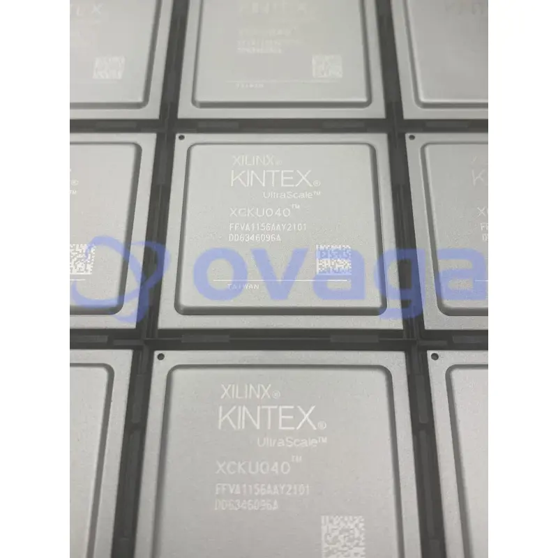
$5000Xilinx XCKU040-2FFVA1156E
Next-generation reconfigurable processor for optimized system architecture


ブランド: Xilinx
製造元部品 #: XCKU040-2FFVA1156E
データシート: XCKU040-2FFVA1156E Datasheet (PDF)
パッケージ/ケース: FCBGA-1156
XCKU040-2FFVA1156E 概要
The advanced features of the XCKU040-2FFVA1156E FPGA make it a powerful tool for engineers seeking to push the boundaries of digital design. With its robust logic resources, high-speed interfaces, and efficient use of resources, this FPGA enables the development of innovative solutions that can meet the demands of modern technology
特徴
- Series: Kintex UltraScale+
- Logic Cells: 363,000
- DSP Slices: 29,400
- Transceivers: 32.5 Gbps
- Device Code: XCKU040-2FFVA11-56E
応用
- Cloud computing
- Audio processing
- Robotics industry

仕様
| パラメータ | 価値 | パラメータ | 価値 |
|---|---|---|---|
| Product Category | FPGA - Field Programmable Gate Array | RoHS | Details |
| Series | XCKU040 | Number of Logic Elements | 530250 LE |
| Adaptive Logic Modules - ALMs | 30300 ALM | Embedded Memory | 21.1 Mbit |
| Number of I/Os | 520 I/O | Supply Voltage - Min | 922 mV |
| Supply Voltage - Max | 979 mV | Minimum Operating Temperature | 0 C |
| Maximum Operating Temperature | + 100 C | Data Rate | 12.5 Gb/s |
| Number of Transceivers | 20 Transceiver | Mounting Style | SMD/SMT |
| Package / Case | FCBGA-1156 | Brand | Xilinx |
| Distributed RAM | 7 Mbit | Embedded Block RAM - EBR | 21.1 Mbit |
| Moisture Sensitive | Yes | Number of Logic Array Blocks - LABs | 30300 LAB |
| Operating Supply Voltage | 850 mV | Product Type | FPGA - Field Programmable Gate Array |
| Factory Pack Quantity | 1 | Subcategory | Programmable Logic ICs |
| Tradename | Kintex UltraScale |
配送
| 配送タイプ | 配送料 | リードタイム | |
|---|---|---|---|
 |
DHL | $20.00-$40.00 (0.50 KG) | 2-5 日々 |
 |
フェデックス | $20.00-$40.00 (0.50 KG) | 2-5 日々 |
 |
UPS | $20.00-$40.00 (0.50 KG) | 2-5 日々 |
 |
TNT | $20.00-$40.00 (0.50 KG) | 2-5 日々 |
 |
EMS | $20.00-$40.00 (0.50 KG) | 2-5 日々 |
 |
登録された航空便 | $20.00-$40.00 (0.50 KG) | 2-5 日々 |
処理時間:送料は地域や国によって異なります。
支払い
| 支払条件 | ハンドフィー | |
|---|---|---|
 |
電信送金 | 銀行手数料 US$30.00 を請求します。 |
 |
ペイパル | 4.0%のサービス料がかかります。 |
 |
クレジットカード | 3.5%のサービス料がかかります。 |
 |
ウエスタンユニオン | charge US.00 banking fee. |
 |
送金サービス | 銀行手数料は 0.00 米ドルかかります。 |
保証
1.購入した電子部品には365日保証が含まれており、製品の品質を保証します。
2.受け取った商品の一部が完璧な品質ではない場合、当社は責任を持って返金または交換を手配します。 ただし、商品は元の状態のままでなければなりません。
パッキング
-

ステップ1 :製品
-

ステップ2 :真空包装
-

ステップ3 :静電気防止袋
-

ステップ4 :個包装
-

ステップ5 :梱包箱
-

ステップ6 :バーコード配送タグ


すべての製品は静電気防止袋に梱包されます。 ESD 帯電防止保護を備えた状態で出荷されます。
社外の ESD 梱包ラベルには、部品番号、ブランド、数量などの当社の情報が使用されます。
私たちは出荷前にすべての商品を検査し、すべての製品が良好な状態であることを確認し、部品が新しいオリジナルでデータシートと一致していることを確認します。
すべての商品に問題がないことを確認した後、梱包後、安全に梱包し、グローバルエクスプレスで発送します。 優れた耐穿刺性と耐引裂性を示し、シールの完全性も良好です。


同等部品
のために XCKU040-2FFVA1156E コンポーネントの場合は、これらの交換部品および代替部品を検討してください:
部品番号
ブランド
パッケージ
説明
部品番号 : XCKU040-2FFVA1156E
ブランド :
パッケージ : 1156-BBGA, FCBGA
説明 : There are no direct equivalent parts numbers for the XCKU040-2FFVA1156E as it is a unique FPGA from Xilinx. However, other FPGAs from Xilinx and other manufacturers may offer similar capabilities and can provide alternative options for specific applications.
パーツポイント
-
The XCKU040-2FFVA1156E chip is a versatile field-programmable gate array (FPGA) that belongs to the Xilinx Kintex UltraScale family. It offers a high-performance and low-power solution for various applications, including data center, networking, and aerospace systems. With its advanced features like high-speed transceivers, configurable logic blocks, and embedded memory, the XCKU040-2FFVA1156E chip provides flexibility and scalability in hardware development.
-
Equivalent
There are no direct equivalent products to the XCKU040-2FFVA1156E chip. However, the Xilinx Virtex UltraScale+ family offers similar FPGA chips with varying features and specifications that may be suitable depending on the specific requirements of the application. -
Features
The features of XCKU040-2FFVA1156E include a Xilinx UltraScale+ FPGA, 965,000 logic cells, 5,520 DSP slices, 16.3 Mb of distributed RAM, 40 Mb of block RAM, 96 gigabit transceivers, and 65,520 CLB flip-flops. It also offers 640 digital I/O pins, PCIe Gen3 support, and up to 4.096 Mbits of integrated synchronous RAM. -
Pinout
The XCKU040-2FFVA1156E is a Field Programmable Gate Array (FPGA) with a pin count of 1156. The function of the FPGA can be customized according to user requirements, as it is programmable and can implement various digital logic functions. -
Manufacturer
The XCKU040-2FFVA1156E is manufactured by Xilinx Inc., a semiconductor company that specializes in the development and production of programmable logic devices and related software tools. -
Application Field
The XCKU040-2FFVA1156E is a Field Programmable Gate Array (FPGA) that can be used in various applications such as data center acceleration, wired communication, wireless infrastructure, industrial automation, and aerospace and defense. It offers high-performance computing, low-power capabilities, and advanced features for these application areas. -
Package
The XCKU040-2FFVA1156E chip is available in a Flip Chip Ball Grid Array (FCBGA) package type. It has a form factor of 1156 pins and a size of 35 mm x 35 mm.


データシート PDF
私たちは高品質の製品、思いやりのあるサービス、販売後の保証を提供します
-

豊富な商品を取り揃えておりますので、お客様の様々なニーズにお応え致します。
-

最小注文数量は1個からとなります。
-

最低国際配送料は0.00ドルから
-

全商品365日品質保証


