

画像は参考用です。製品仕様を参照してください。
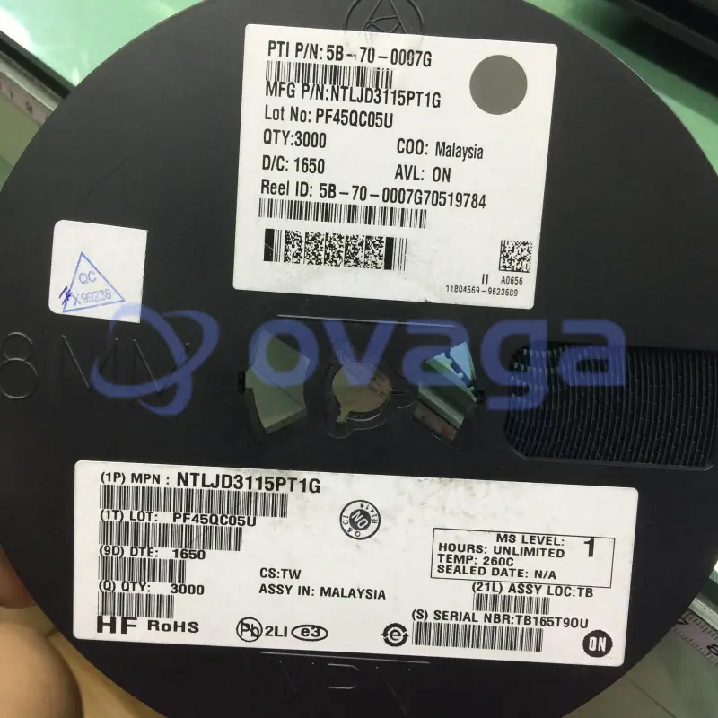
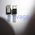
ON NTLJD3115PT1G
Mosfet Array 20V 2.3A 710mW Surface Mount 6-WDFN (2x2)


ブランド: ON Semiconductor, LLC
製造元部品 #: NTLJD3115PT1G
データシート: NTLJD3115PT1G Datasheet (PDF)
パッケージ/ケース: WDFN EP
製品の種類: トランジスタ
NTLJD3115PT1G 概要
Mosfet Array 20V 2.3A 710mW Surface Mount 6-WDFN (2x2)
特徴
- WDFN Package Provides Exposed Drain Pad for Excellent Thermal Conduction
- 2x2 mm Footprint Same as SC-88
- Lowest RDS(on) Solution in 2x2 mm Package
- 1.8 V RDS(on) Rating for Operation at Low Voltage Gate Drive Logic Level
- Low Profile (< 0.8 mm) for Easy Fit in Thin Environments
- Bidirectional Current Flow with Common Source Configuration
応用
- Optimized for Battery and Load Management Applications in Portable Equipment
- Li-Ion Battery Charging and Protection Circuits
- High Side Load Switch
仕様
| パラメータ | 価値 | パラメータ | 価値 |
|---|---|---|---|
| Source Content uid | NTLJD3115PT1G | Pbfree Code | Yes |
| Part Life Cycle Code | Active | Ihs Manufacturer | ONSEMI |
| Part Package Code | WDFN6 2x2, 0.65P | Package Description | WDFN-6 |
| Pin Count | 6 | Manufacturer Package Code | 506AN |
| Reach Compliance Code | compliant | ECCN Code | EAR99 |
| Factory Lead Time | 22 Weeks | Samacsys Manufacturer | onsemi |
| Additional Feature | LOGIC LEVEL COMPATIBLE | Case Connection | DRAIN |
| Configuration | SEPARATE, 2 ELEMENTS WITH BUILT-IN DIODE | DS Breakdown Voltage-Min | 20 V |
| Drain Current-Max (ID) | 2.3 A | Drain-source On Resistance-Max | 0.135 Ω |
| FET Technology | METAL-OXIDE SEMICONDUCTOR | JESD-30 Code | S-PDSO-N6 |
| JESD-609 Code | e3 | Moisture Sensitivity Level | 1 |
| Number of Elements | 1 | Number of Terminals | 6 |
| Operating Mode | ENHANCEMENT MODE | Operating Temperature-Max | 150 °C |
| Operating Temperature-Min | -55 °C | Package Body Material | PLASTIC/EPOXY |
| Package Shape | RECTANGULAR | Package Style | SMALL OUTLINE |
| Peak Reflow Temperature (Cel) | 260 | Polarity/Channel Type | P-CHANNEL |
| Power Dissipation-Max (Abs) | 1.5 W | Pulsed Drain Current-Max (IDM) | 20 A |
| Qualification Status | Not Qualified | Surface Mount | YES |
| Terminal Finish | MATTE TIN | Terminal Form | NO LEAD |
| Terminal Position | DUAL | Time@Peak Reflow Temperature-Max (s) | 30 |
| Transistor Application | SWITCHING | Transistor Element Material | SILICON |
| feature-category | Power MOSFET | feature-material | |
| feature-process-technology | feature-configuration | Dual | |
| feature-channel-mode | Enhancement | feature-channel-type | P |
| feature-number-of-elements-per-chip | 2 | feature-maximum-drain-source-voltage-v | 20 |
| feature-maximum-gate-source-voltage-v | ±8 | feature-maximum-gate-threshold-voltage-v | 1 |
| feature-maximum-continuous-drain-current-a | 3.3 | feature-maximum-drain-source-resistance-mohm | [email protected] |
| feature-typical-gate-charge-vgs-nc | [email protected] | feature-typical-gate-charge-10v-nc | 5.5 |
| feature-typical-input-capacitance-vds-pf | 531@10V | feature-typical-output-capacitance-pf | 91 |
| feature-maximum-power-dissipation-mw | 2300 | feature-packaging | Tape and Reel |
| feature-rad-hard | feature-pin-count | 6 | |
| feature-supplier-package | WDFN EP | feature-standard-package-name1 | DFN |
| feature-cecc-qualified | No | feature-esd-protection | |
| feature-military | No | feature-aec-qualified | No |
| feature-aec-qualified-number | feature-auto-motive | No | |
| feature-p-pap | No | feature-eccn-code | EAR99 |
| feature-svhc | No |
配送
| 配送タイプ | 配送料 | リードタイム | |
|---|---|---|---|
 |
DHL | $20.00-$40.00 (0.50 KG) | 2-5 日々 |
 |
フェデックス | $20.00-$40.00 (0.50 KG) | 2-5 日々 |
 |
UPS | $20.00-$40.00 (0.50 KG) | 2-5 日々 |
 |
TNT | $20.00-$40.00 (0.50 KG) | 2-5 日々 |
 |
EMS | $20.00-$40.00 (0.50 KG) | 2-5 日々 |
 |
登録された航空便 | $20.00-$40.00 (0.50 KG) | 2-5 日々 |
処理時間:送料は地域や国によって異なります。
支払い
| 支払条件 | ハンドフィー | |
|---|---|---|
 |
電信送金 | 銀行手数料 US$30.00 を請求します。 |
 |
ペイパル | 4.0%のサービス料がかかります。 |
 |
クレジットカード | 3.5%のサービス料がかかります。 |
 |
ウエスタンユニオン | charge US.00 banking fee. |
 |
送金サービス | 銀行手数料は 0.00 米ドルかかります。 |
保証
1.購入した電子部品には365日保証が含まれており、製品の品質を保証します。
2.受け取った商品の一部が完璧な品質ではない場合、当社は責任を持って返金または交換を手配します。 ただし、商品は元の状態のままでなければなりません。
パッキング
-

ステップ1 :製品
-

ステップ2 :真空包装
-

ステップ3 :静電気防止袋
-

ステップ4 :個包装
-

ステップ5 :梱包箱
-

ステップ6 :バーコード配送タグ


すべての製品は静電気防止袋に梱包されます。 ESD 帯電防止保護を備えた状態で出荷されます。
社外の ESD 梱包ラベルには、部品番号、ブランド、数量などの当社の情報が使用されます。
私たちは出荷前にすべての商品を検査し、すべての製品が良好な状態であることを確認し、部品が新しいオリジナルでデータシートと一致していることを確認します。
すべての商品に問題がないことを確認した後、梱包後、安全に梱包し、グローバルエクスプレスで発送します。 優れた耐穿刺性と耐引裂性を示し、シールの完全性も良好です。


パーツポイント
-
The NTLJD3115PT1G chip is a high-speed, low voltage dual N-channel MOSFET designed for applications such as load and motor control. It has a compact 2mm x 2mm package and features low on-resistance with fast switching capabilities. This chip is suitable for use in a variety of electronic devices that require efficient power management and control.
-
Features
The NTLJD3115PT1G is a high-performance N-channel MOSFET transistor. It has a low on-resistance, high power dissipation capability, and is designed for applications requiring high efficiency power conversion. The device offers low gate charge which enables faster switching, making it suitable for various applications including power supplies, motor controls, and automotive systems. -
Pinout
The NTLJD3115PT1G is a MOSFET transistor with a 6-pin DFN package. It is a dual N-Channel enhancement mode transistor designed for low voltage, high-speed switching applications. The pin count includes 3 pins per channel: drain, source, and gate for each N-Channel. -
Manufacturer
The manufacturer of the NTLJD3115PT1G is ON Semiconductor. It is a semiconductor manufacturing company that specializes in designing and producing a wide range of integrated circuits, power management solutions, and discrete components for various industries including automotive, communications, consumer electronics, and industrial applications. -
Application Field
The NTLJD3115PT1G is a low on-resistance single-channel logic level N-channel MOSFET. It can be used in a variety of applications, including power management, load switching, battery charging, and motor control. Its compact package and high efficiency make it suitable for portable electronics, automotive systems, industrial equipment, and more. -
Package
The NTLJD3115PT1G chip is available in a surface mount package type known as SOT-563. It is a small form factor package with dimensions measuring approximately 1.6mm x 1.6mm x 0.6mm.


データシート PDF
私たちは高品質の製品、思いやりのあるサービス、販売後の保証を提供します
-

豊富な商品を取り揃えておりますので、お客様の様々なニーズにお応え致します。
-

最小注文数量は1個からとなります。
-

最低国際配送料は0.00ドルから
-

全商品365日品質保証


Shipping was prompt and efficient.