

画像は参考用です。製品仕様を参照してください。
ON FDS89161
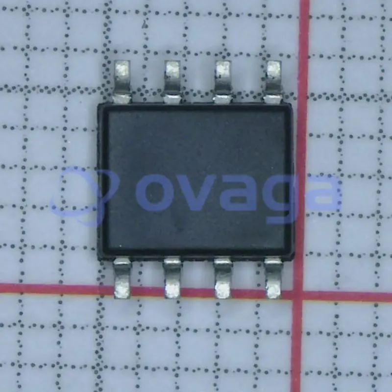
Mosfet Array 100V 2.7A 1.6W Surface Mount 8-SOIC


ブランド: ON Semiconductor, LLC
製造元部品 #: FDS89161
データシート: FDS89161 Datasheet (PDF)
パッケージ/ケース: SO-8
製品の種類: トランジスタ
FDS89161 概要
This N-Channel MOSFET is produced using an advanced Power Trench® process that has been optimized for rDS(on), switching performance and ruggedness.
特徴
- Shielded Gate MOSFET Technology
- Max rDS(on) = 105 mΩat VGS= 10 V, ID = 2.7 A
- Max rDS(on) = 171 mΩ at VGS = 6 V, ID = 2.1 A
- High performance trench technology for extremely low rDS(on)
- High power and current handling capability in a widely used surface mount package
- 100% UIL Tested
- RoHS Compliant
応用
- This product is general usage and suitable for many different applications.
- Synchronous Rectifier
- Primary Switch for Bridge Topology
仕様
| パラメータ | 価値 | パラメータ | 価値 |
|---|---|---|---|
| Source Content uid | FDS89161 | Pbfree Code | Yes |
| Part Life Cycle Code | Active | Ihs Manufacturer | ONSEMI |
| Package Description | SOP-8 | Manufacturer Package Code | 751EB |
| Reach Compliance Code | compliant | ECCN Code | EAR99 |
| Factory Lead Time | 24 Weeks | Samacsys Manufacturer | onsemi |
| Application | SWITCHING | Configuration | SEPARATE, 2 ELEMENTS WITH BUILT-IN DIODE |
| FET Technology | METAL-OXIDE SEMICONDUCTOR | JESD-30 Code | R-PDSO-G8 |
| Moisture Sensitivity Level | 1 | Number of Elements | 2 |
| Number of Terminals | 8 | Operating Mode | ENHANCEMENT MODE |
| Package Body Material | PLASTIC/EPOXY | Package Shape | RECTANGULAR |
| Package Style | SMALL OUTLINE | Peak Reflow Temperature (Cel) | 260 |
| Polarity/Channel Type | N-CHANNEL | Surface Mount | YES |
| Terminal Finish | MATTE TIN | Terminal Form | GULL WING |
| Terminal Position | DUAL | Time@Peak Reflow Temperature-Max (s) | 30 |
| Transistor Element Material | SILICON | feature-category | Power MOSFET |
| feature-material | feature-process-technology | TMOS | |
| feature-configuration | Dual Dual Drain | feature-channel-mode | Enhancement |
| feature-channel-type | N | feature-number-of-elements-per-chip | 2 |
| feature-maximum-drain-source-voltage-v | 100 | feature-maximum-gate-source-voltage-v | ±20 |
| feature-maximum-gate-threshold-voltage-v | feature-maximum-continuous-drain-current-a | 2.7 | |
| feature-maximum-drain-source-resistance-mohm | 105@10V | feature-typical-gate-charge-vgs-nc | 3@10V|1.7@5V |
| feature-typical-gate-charge-10v-nc | 3 | feature-typical-input-capacitance-vds-pf | 158@50V |
| feature-typical-output-capacitance-pf | feature-maximum-power-dissipation-mw | 1600 | |
| feature-packaging | Tape and Reel | feature-rad-hard | |
| feature-pin-count | 8 | feature-supplier-package | SOIC |
| feature-standard-package-name1 | SO | feature-cecc-qualified | No |
| feature-esd-protection | feature-military | No | |
| feature-aec-qualified | No | feature-aec-qualified-number | |
| feature-auto-motive | No | feature-p-pap | No |
| feature-eccn-code | EAR99 | feature-svhc | No |
| feature-svhc-exceeds-threshold | No |
配送
| 配送タイプ | 配送料 | リードタイム | |
|---|---|---|---|
 |
DHL | $20.00-$40.00 (0.50 KG) | 2-5 日々 |
 |
フェデックス | $20.00-$40.00 (0.50 KG) | 2-5 日々 |
 |
UPS | $20.00-$40.00 (0.50 KG) | 2-5 日々 |
 |
TNT | $20.00-$40.00 (0.50 KG) | 2-5 日々 |
 |
EMS | $20.00-$40.00 (0.50 KG) | 2-5 日々 |
 |
登録された航空便 | $20.00-$40.00 (0.50 KG) | 2-5 日々 |
処理時間:送料は地域や国によって異なります。
支払い
| 支払条件 | ハンドフィー | |
|---|---|---|
 |
電信送金 | 銀行手数料 US$30.00 を請求します。 |
 |
ペイパル | 4.0%のサービス料がかかります。 |
 |
クレジットカード | 3.5%のサービス料がかかります。 |
 |
ウエスタンユニオン | charge US.00 banking fee. |
 |
送金サービス | 銀行手数料は 0.00 米ドルかかります。 |
保証
1.購入した電子部品には365日保証が含まれており、製品の品質を保証します。
2.受け取った商品の一部が完璧な品質ではない場合、当社は責任を持って返金または交換を手配します。 ただし、商品は元の状態のままでなければなりません。
パッキング
-

ステップ1 :製品
-

ステップ2 :真空包装
-

ステップ3 :静電気防止袋
-

ステップ4 :個包装
-

ステップ5 :梱包箱
-

ステップ6 :バーコード配送タグ


すべての製品は静電気防止袋に梱包されます。 ESD 帯電防止保護を備えた状態で出荷されます。
社外の ESD 梱包ラベルには、部品番号、ブランド、数量などの当社の情報が使用されます。
私たちは出荷前にすべての商品を検査し、すべての製品が良好な状態であることを確認し、部品が新しいオリジナルでデータシートと一致していることを確認します。
すべての商品に問題がないことを確認した後、梱包後、安全に梱包し、グローバルエクスプレスで発送します。 優れた耐穿刺性と耐引裂性を示し、シールの完全性も良好です。


パーツポイント
-
The FDS89161 chip is a high-performance integrated circuit designed for use in various electronic devices. It offers advanced features such as low power consumption, high-speed data processing, and compatibility with different communication protocols. The chip's versatility and efficiency make it suitable for applications in areas like consumer electronics, automotive systems, and industrial control.
-
Features
The FDS89161 is a semiconductor device designed for power management solutions. It features a low on-resistance, allowing for efficient power delivery. It also has a low gate charge, making it suitable for fast switching applications. Additionally, it offers a small package size, enabling space-saving designs. -
Pinout
The FDS89161 is a dual N-channel PowerTrench MOSFET with a pin count of 8. Its functions include providing low on-resistance and high-speed switching capabilities in applications such as power management circuits, motor drives, and load switches. -
Manufacturer
The manufacturer of the FDS89161 is Fairchild Semiconductor. Fairchild Semiconductor is a global company that designs, develops, and manufactures semiconductor products. They specialize in power and signal path products for various applications in automotive, industrial, and consumer markets. -
Application Field
The FDS89161 is a high-voltage power MOSFET designed for applications requiring efficient power switching in a small yet robust package. With a high drain-source breakdown voltage and low on-resistance, it is commonly used in a variety of applications such as motor control, power supplies, LED lighting, and battery charging circuits. -
Package
The FDS89161 chip is available in a package type of QFN (Quad Flat No-Lead), with a form factor of 6x6mm and a size of 36 mm².


データシート PDF
私たちは高品質の製品、思いやりのあるサービス、販売後の保証を提供します
-

豊富な商品を取り揃えておりますので、お客様の様々なニーズにお応え致します。
-

最小注文数量は1個からとなります。
-

最低国際配送料は0.00ドルから
-

全商品365日品質保証


Excellent service and quality make Ovaga a top choice for electronic components.