画像は参考用です。製品仕様を参照してください。
ON FDC6321C

Mosfet Array 25V 680mA, 460mA 700mW Surface Mount SuperSOT™-6


ブランド: ON
製造元部品 #: FDC6321C
データシート: FDC6321C データシート (PDF)
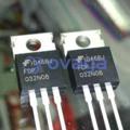
パッケージ/ケース: SOT23-6
RoHS ステータス:
在庫状況: 3000 個、新しいオリジナル
製品の種類: 金属酸化物半導体フィールド効果トランジスタ(MOSFET)
Warranty: 1 Year Ovaga Warranty - Find Out More
0
1
*すべての価格は米ドルです
| 数量 | 単価 | 外部価格 |
|---|---|---|
| 1 | $0.373 | $0.373 |
| 10 | $0.305 | $3.050 |
| 30 | $0.275 | $8.250 |
| 100 | $0.238 | $23.800 |
| 500 | $0.222 | $111.000 |
| 1000 | $0.214 | $214.000 |
In Stock:3000 PCS
FDC6321C 概要
These dual N & P Channel logic level enhancement mode field effect transistors are produced using a proprietary, high cell density, DMOS technology. This very high density process is especially tailored to minimize on-state resistance. This device has been designed especially for low voltage applications as a replacement for digital transistors in load switching applications. Since bias resistors are not required this dual digital FET can replace several digital transistors with different bias resistors.
特徴
- N-Ch 25 V, 0.68 A, RDS(ON) = 0.45 Ω @ VGS= 4.5 V
- P-Ch -25 V, -0.46 A, RDS(ON) = 1.1 Ω @ VGS= -4.5 V.
- Very low level gate drive requirements allowing direct operation in 3 V circuits. VGS(th) < 1.0V.
- Gate-Source Zener for ESD ruggedness. >6kV Human Body Model
- Replace multiple dual NPN & PNP digital transistors.
応用
- This product is general usage and suitable for many different applications.
仕様
| パラメータ | 価値 | パラメータ | 価値 |
|---|---|---|---|
| Product Category | MOSFET | RoHS | Details |
| Technology | Si | Mounting Style | SMD/SMT |
| Package / Case | SSOT-6 | Transistor Polarity | N-Channel, P-Channel |
| Number of Channels | 2 Channel | Vds - Drain-Source Breakdown Voltage | 25 V |
| Id - Continuous Drain Current | 680 mA, 460 mA | Rds On - Drain-Source Resistance | 450 mOhms |
| Vgs - Gate-Source Voltage | - 8 V, + 8 V | Vgs th - Gate-Source Threshold Voltage | 650 mV, 1.5 V |
| Qg - Gate Charge | 2.3 nC, 1.5 nC | Minimum Operating Temperature | - 55 C |
| Maximum Operating Temperature | + 150 C | Pd - Power Dissipation | 900 mW |
| Channel Mode | Enhancement | Series | FDC6321C |
| Brand | onsemi / Fairchild | Configuration | Dual |
| Fall Time | 8 ns, 9 ns | Forward Transconductance - Min | 1.45 S, 0.8 S |
| Height | 1.1 mm | Length | 2.9 mm |
| Product | MOSFET Small Signals | Product Type | MOSFET |
| Rise Time | 8 ns, 9 ns | Factory Pack Quantity | 3000 |
| Subcategory | MOSFETs | Transistor Type | 1 N-Channel, 1 P-Channel |
| Type | FET | Typical Turn-Off Delay Time | 17 ns, 55 ns |
| Typical Turn-On Delay Time | 3 ns, 7 ns | Width | 1.6 mm |
| Part # Aliases | FDC6321C_NL |
配送
| 配送タイプ | 配送料 | リードタイム | |
|---|---|---|---|
 |
DHL | $20.00-$40.00 (0.50 KG) | 2-5 日々 |
 |
フェデックス | $20.00-$40.00 (0.50 KG) | 2-5 日々 |
 |
UPS | $20.00-$40.00 (0.50 KG) | 2-5 日々 |
 |
TNT | $20.00-$40.00 (0.50 KG) | 2-5 日々 |
 |
EMS | $20.00-$40.00 (0.50 KG) | 2-5 日々 |
 |
登録された航空便 | $20.00-$40.00 (0.50 KG) | 2-5 日々 |
処理時間:送料は地域や国によって異なります。
支払い
| 支払条件 | ハンドフィー | |
|---|---|---|
 |
電信送金 | 銀行手数料 US$30.00 を請求します。 |
 |
ペイパル | 4.0%のサービス料がかかります。 |
 |
クレジットカード | 3.5%のサービス料がかかります。 |
 |
ウエスタンユニオン | charge US.00 banking fee. |
 |
送金サービス | 銀行手数料は 0.00 米ドルかかります。 |
保証
1.購入した電子部品には365日保証が含まれており、製品の品質を保証します。
2.受け取った商品の一部が完璧な品質ではない場合、当社は責任を持って返金または交換を手配します。 ただし、商品は元の状態のままでなければなりません。
パッキング
-

ステップ1 :製品
-

ステップ2 :真空包装
-

ステップ3 :静電気防止袋
-

ステップ4 :個包装
-

ステップ5 :梱包箱
-

ステップ6 :バーコード配送タグ


すべての製品は静電気防止袋に梱包されます。 ESD 帯電防止保護を備えた状態で出荷されます。
社外の ESD 梱包ラベルには、部品番号、ブランド、数量などの当社の情報が使用されます。
私たちは出荷前にすべての商品を検査し、すべての製品が良好な状態であることを確認し、部品が新しいオリジナルでデータシートと一致していることを確認します。
すべての商品に問題がないことを確認した後、梱包後、安全に梱包し、グローバルエクスプレスで発送します。 優れた耐穿刺性と耐引裂性を示し、シールの完全性も良好です。


パーツポイント
-
The FDC6321C chip is an integrated circuit that combines an analog front end with a digital interface for capacitance-to-digital conversion. It is used for proximity sensing, touch detection, and liquid level sensing applications. The chip provides accurate and stable measurements with low power consumption, making it suitable for various industrial and consumer electronic devices.
-
Features
The FDC6321C features a low on-resistance, allowing for efficient power handling. It has a low gate charge, enabling quick switching performance. The device also boasts a low threshold voltage, making it ideal for low-voltage applications. Offering high electrical performance in a compact form factor, the FDC6321C is suitable for a range of power control applications. -
Pinout
The FDC6321C is a dual-channel power MOSFET driver. It has 8 pins (VCC, GND, IN1, IN2, OUT1, OUT2, UVLO, and VDS). Its main function is to provide a high voltage and high current drive capability to switch power MOSFETs in various applications, such as DC-DC converters, motor drivers, and inverters. -
Manufacturer
The FDC6321C is manufactured by Fairchild Semiconductor. Fairchild Semiconductor is an American company that specializes in the design, development, and production of a wide range of semiconductor devices. They provide innovative solutions for various industries, including automotive, consumer electronics, telecommunications, and more. -
Application Field
The FDC6321C is a high-precision capacitance-to-digital converter that can be used in a variety of applications, including touch sensing, level sensing, proximity sensing, and liquid and gas flow sensing. It can also be used in industrial automation, consumer electronics, automotive, and medical devices. -
Package
The FDC6321C chip is available in a SOT-23-6 package, which has 6 surface-mount pins.


私たちは高品質の製品、思いやりのあるサービス、販売後の保証を提供します
-

豊富な商品を取り揃えておりますので、お客様の様々なニーズにお応え致します。
-

最小注文数量は1個からとなります。
-

最低国際配送料は0.00ドルから
-

全商品365日品質保証