

画像は参考用です。製品仕様を参照してください。
ON FDB52N20TM
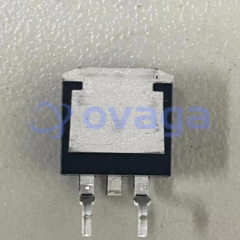
N-Channel 200 V 52A (Tc) 357W (Tc) Surface Mount TO-263 (D2PAK)


ブランド: ON Semiconductor, LLC
製造元部品 #: FDB52N20TM
データシート: FDB52N20TM Datasheet (PDF)
パッケージ/ケース: D2PAK
製品の種類: トランジスタ
FDB52N20TM 概要
UniFETTM MOSFET is a high voltage MOSFET family based on planar stripe and DMOS technology. This MOSFET is tailored to reduce on-state resistance, and to provide better switching performance and higher avalanche energy strength. This device family is suitable for switching power converter applications such as power factor correction (PFC), flat panel display (FPD) TV power, ATX and electronic lamp ballasts.
特徴
- RDS(on) = 49mΩ ( Max.)@ VGS = 10V, ID = 26A
- Low gate charge ( Typ. 49nC)
- Low Crss ( Typ. 66pF)
- 100% avalanche tested
応用
- This product is general usage and suitable for many different applications.
仕様
| パラメータ | 価値 | パラメータ | 価値 |
|---|---|---|---|
| Source Content uid | FDB52N20TM | Pbfree Code | Yes |
| Part Life Cycle Code | Active | Ihs Manufacturer | ONSEMI |
| Package Description | D2PAK-3/2 | Manufacturer Package Code | 418AJ |
| Reach Compliance Code | not_compliant | ECCN Code | EAR99 |
| Factory Lead Time | 10 Weeks | Samacsys Manufacturer | onsemi |
| Avalanche Energy Rating (Eas) | 2520 mJ | Case Connection | DRAIN |
| Configuration | SINGLE WITH BUILT-IN DIODE | DS Breakdown Voltage-Min | 200 V |
| Drain Current-Max (ID) | 52 A | Drain-source On Resistance-Max | 0.049 Ω |
| FET Technology | METAL-OXIDE SEMICONDUCTOR | JEDEC-95 Code | TO-263 |
| JESD-30 Code | R-PSSO-G2 | JESD-609 Code | e3 |
| Moisture Sensitivity Level | 1 | Number of Elements | 1 |
| Number of Terminals | 2 | Operating Mode | ENHANCEMENT MODE |
| Operating Temperature-Max | 150 °C | Operating Temperature-Min | -55 °C |
| Package Body Material | PLASTIC/EPOXY | Package Shape | RECTANGULAR |
| Package Style | SMALL OUTLINE | Peak Reflow Temperature (Cel) | 245 |
| Polarity/Channel Type | N-CHANNEL | Power Dissipation-Max (Abs) | 357 W |
| Pulsed Drain Current-Max (IDM) | 208 A | Qualification Status | Not Qualified |
| Surface Mount | YES | Terminal Finish | Matte Tin (Sn) - annealed |
| Terminal Form | GULL WING | Terminal Position | SINGLE |
| Time@Peak Reflow Temperature-Max (s) | 30 | Transistor Application | SWITCHING |
| Transistor Element Material | SILICON | feature-category | Power MOSFET |
| feature-material | feature-process-technology | UniFET | |
| feature-configuration | Single | feature-channel-mode | Enhancement |
| feature-channel-type | N | feature-number-of-elements-per-chip | 1 |
| feature-maximum-drain-source-voltage-v | 200 | feature-maximum-gate-source-voltage-v | ±30 |
| feature-maximum-gate-threshold-voltage-v | feature-maximum-continuous-drain-current-a | 52 | |
| feature-maximum-drain-source-resistance-mohm | 49@10V | feature-typical-gate-charge-vgs-nc | 49@10V |
| feature-typical-gate-charge-10v-nc | 49 | feature-typical-input-capacitance-vds-pf | 2230@25V |
| feature-typical-output-capacitance-pf | feature-maximum-power-dissipation-mw | 357000 | |
| feature-packaging | Tape and Reel | feature-rad-hard | |
| feature-pin-count | 3 | feature-supplier-package | D2PAK |
| feature-standard-package-name1 | TO-263 | feature-cecc-qualified | No |
| feature-esd-protection | feature-military | No | |
| feature-aec-qualified | No | feature-aec-qualified-number | |
| feature-auto-motive | No | feature-p-pap | No |
| feature-eccn-code | EAR99 | feature-svhc | Yes |
| feature-svhc-exceeds-threshold | Yes |
配送
| 配送タイプ | 配送料 | リードタイム | |
|---|---|---|---|
 |
DHL | $20.00-$40.00 (0.50 KG) | 2-5 日々 |
 |
フェデックス | $20.00-$40.00 (0.50 KG) | 2-5 日々 |
 |
UPS | $20.00-$40.00 (0.50 KG) | 2-5 日々 |
 |
TNT | $20.00-$40.00 (0.50 KG) | 2-5 日々 |
 |
EMS | $20.00-$40.00 (0.50 KG) | 2-5 日々 |
 |
登録された航空便 | $20.00-$40.00 (0.50 KG) | 2-5 日々 |
処理時間:送料は地域や国によって異なります。
支払い
| 支払条件 | ハンドフィー | |
|---|---|---|
 |
電信送金 | 銀行手数料 US$30.00 を請求します。 |
 |
ペイパル | 4.0%のサービス料がかかります。 |
 |
クレジットカード | 3.5%のサービス料がかかります。 |
 |
ウエスタンユニオン | charge US.00 banking fee. |
 |
送金サービス | 銀行手数料は 0.00 米ドルかかります。 |
保証
1.購入した電子部品には365日保証が含まれており、製品の品質を保証します。
2.受け取った商品の一部が完璧な品質ではない場合、当社は責任を持って返金または交換を手配します。 ただし、商品は元の状態のままでなければなりません。
パッキング
-

ステップ1 :製品
-

ステップ2 :真空包装
-

ステップ3 :静電気防止袋
-

ステップ4 :個包装
-

ステップ5 :梱包箱
-

ステップ6 :バーコード配送タグ


すべての製品は静電気防止袋に梱包されます。 ESD 帯電防止保護を備えた状態で出荷されます。
社外の ESD 梱包ラベルには、部品番号、ブランド、数量などの当社の情報が使用されます。
私たちは出荷前にすべての商品を検査し、すべての製品が良好な状態であることを確認し、部品が新しいオリジナルでデータシートと一致していることを確認します。
すべての商品に問題がないことを確認した後、梱包後、安全に梱包し、グローバルエクスプレスで発送します。 優れた耐穿刺性と耐引裂性を示し、シールの完全性も良好です。


パーツポイント
-
The FDB52N20TM is a power MOSFET chip designed for various electronic applications. It has a high voltage rating of 200V and a continuous drain current of 52A, making it suitable for power switch devices. The chip features low on-resistance and fast switching capabilities, providing efficient power conversion. Its compact size and durability make it an ideal choice for automotive, industrial, and consumer electronics.
-
Equivalent
Some equivalent products of the FDB52N20TM chip are the IRFP250N and the IRFB11N50A. -
Features
The features of FDB52N20TM include N-channel MOSFET technology, a drain-source voltage of 200V, a continuous drain current of 52A, a low on-state resistance of 36mΩ, and a fast switching speed. It is suitable for various applications, including power supplies, motor drives, and inverters. -
Pinout
The FDB52N20TM is a MOSFET transistor with a TO-263 package, consisting of 3 pins. Pin 1 is the gate, pin 2 is the drain, and pin 3 is the source. It is commonly used in power electronic applications due to its high voltage and current handling capabilities. -
Manufacturer
The manufacturer of the FDB52N20TM is Fairchild Semiconductor. It is an American company that specializes in the design, development, and manufacturing of power management solutions. It offers a wide range of products including discrete semiconductors, integrated circuits, and optoelectronics for various industries such as automotive, industrial, and telecommunication. -
Application Field
The FDB52N20TM transistor is commonly used in various applications such as motor control, power supplies, and audio amplifier circuits. Additionally, it is suitable for use in high-speed switching applications due to its low resistance and fast-switching capability. -
Package
The FDB52N20TM chip is available in TO-263 package type. It has a form of a flat, rectangular shape with three leads. The size dimensions of the package are typically around 10mm x 10mm x 2mm.


データシート PDF
私たちは高品質の製品、思いやりのあるサービス、販売後の保証を提供します
-

豊富な商品を取り揃えておりますので、お客様の様々なニーズにお応え致します。
-

最小注文数量は1個からとなります。
-

最低国際配送料は0.00ドルから
-

全商品365日品質保証


Ovaga's components helped me create a product that impressed my clients.