

画像は参考用です。製品仕様を参照してください。
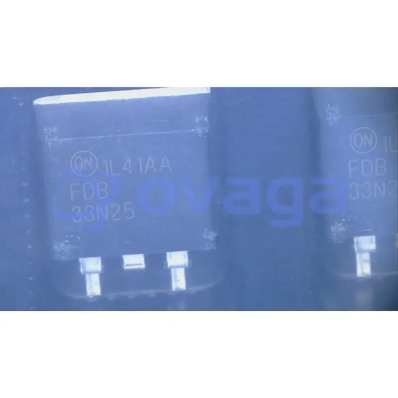
ON FDB33N25TM

D2PAK-packaged Power MOSFET with N-Channel configuration and UniFETTM technology


ブランド: Onsemi
製造元部品 #: FDB33N25TM
データシート: FDB33N25TM Datasheet (PDF)
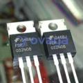
パッケージ/ケース: D2PAK-3 , TO-263-2
RoHS ステータス:
在庫状況: 2161 個、新しいオリジナル
製品の種類: トランジスタ
Warranty: 1 Year Ovaga Warranty - Find Out More
0
1
*すべての価格は米ドルです
| 数量 | 単価 | 外部価格 |
|---|---|---|
| 1 | $1.804 | $1.804 |
| 10 | $1.552 | $15.520 |
| 30 | $1.396 | $41.880 |
| 100 | $1.236 | $123.600 |
| 500 | $1.099 | $549.500 |
| 800 | $1.068 | $854.400 |
In Stock:2161 PCS
FDB33N25TM 概要
UniFETTM MOSFET is a high voltage MOSFET family based on planar stripe and DMOS technology. This MOSFET is tailored to reduce on-state resistance, and to provide better switching performance and higher avalanche energy strength. This device family is suitable for switching power converter applications such as power factor correction (PFC), flat panel display (FPD) TV power, ATX and electronic lamp ballasts.
特徴
Type: N-Channel MOSFET
Voltage Rating (VDS): 250 volts
Current Rating (ID): 33 amperes
RDS(on) (On-State Resistance): This value indicates the resistance between the drain and source when the MOSFET is in the "on" state.
Package: TO-263 (also known as D²PAK or DDPAK) which is a surface-mount package.
Gate Threshold Voltage (VGS(th)): The voltage at which the MOSFET begins to turn on.
応用
- This product is general usage and suitable for many different applications.
仕様
| パラメータ | 価値 | パラメータ | 価値 |
|---|---|---|---|
| Product Name | FDB33N25TM | Product Type | Power MOSFET |
| Manufacturer | ON Semiconductor | Transistor Type | N-Channel |
| Drain-Source Voltage (Vdss) | 250V | Continuous Drain Current (Id) | 33A |
| Rds(on) (On-Resistance) | 0.095 ohms (max) | Gate-Source Threshold Voltage (Vgs(th)) | 2V (max) |
| Operating Temperature Range | -55°C to +175°C | Package / Case | TO-263 (D2PAK) |
| Packaging | Tape & Reel, Tube, and other options | feature-category | Power MOSFET |
| feature-material | feature-process-technology | UniFET | |
| feature-configuration | Single | feature-channel-mode | Enhancement |
| feature-channel-type | N | feature-number-of-elements-per-chip | 1 |
| feature-maximum-drain-source-voltage-v | 250 | feature-maximum-gate-source-voltage-v | ±30 |
| feature-maximum-gate-threshold-voltage-v | 5 | feature-maximum-continuous-drain-current-a | 33 |
| feature-maximum-drain-source-resistance-mohm | 94@10V | feature-typical-gate-charge-vgs-nc | 36.8@10V |
| feature-typical-gate-charge-10v-nc | 36.8 | feature-typical-input-capacitance-vds-pf | 1640@25V |
| feature-typical-output-capacitance-pf | feature-maximum-power-dissipation-mw | 235000 | |
| feature-packaging | Tape and Reel | feature-rad-hard | |
| feature-pin-count | 3 | feature-supplier-package | D2PAK |
| feature-standard-package-name1 | TO-263 | feature-cecc-qualified | No |
| feature-esd-protection | feature-military | No | |
| feature-aec-qualified | No | feature-aec-qualified-number | |
| feature-auto-motive | No | feature-p-pap | No |
| feature-eccn-code | EAR99 | feature-svhc | Yes |
| feature-svhc-exceeds-threshold | Yes | Series | UniFET™ |
| Product Status | Active | FET Type | N-Channel |
| Technology | MOSFET (Metal Oxide) | Drain to Source Voltage (Vdss) | 250 V |
| Current - Continuous Drain (Id) @ 25°C | 33A (Tc) | Drive Voltage (Max Rds On, Min Rds On) | 10V |
| Rds On (Max) @ Id, Vgs | 94mOhm @ 16.5A, 10V | Vgs(th) (Max) @ Id | 5V @ 250µA |
| Gate Charge (Qg) (Max) @ Vgs | 48 nC @ 10 V | Vgs (Max) | ±30V |
| Input Capacitance (Ciss) (Max) @ Vds | 2135 pF @ 25 V | Power Dissipation (Max) | 235W (Tc) |
| Operating Temperature | -55°C ~ 150°C (TJ) | Mounting Type | Surface Mount |
| Supplier Device Package | TO-263 (D2PAK) |
配送
| 配送タイプ | 配送料 | リードタイム | |
|---|---|---|---|
 |
DHL | $20.00-$40.00 (0.50 KG) | 2-5 日々 |
 |
フェデックス | $20.00-$40.00 (0.50 KG) | 2-5 日々 |
 |
UPS | $20.00-$40.00 (0.50 KG) | 2-5 日々 |
 |
TNT | $20.00-$40.00 (0.50 KG) | 2-5 日々 |
 |
EMS | $20.00-$40.00 (0.50 KG) | 2-5 日々 |
 |
登録された航空便 | $20.00-$40.00 (0.50 KG) | 2-5 日々 |
処理時間:送料は地域や国によって異なります。
支払い
| 支払条件 | ハンドフィー | |
|---|---|---|
 |
電信送金 | 銀行手数料 US$30.00 を請求します。 |
 |
ペイパル | 4.0%のサービス料がかかります。 |
 |
クレジットカード | 3.5%のサービス料がかかります。 |
 |
ウエスタンユニオン | charge US.00 banking fee. |
 |
送金サービス | 銀行手数料は 0.00 米ドルかかります。 |
保証
1.購入した電子部品には365日保証が含まれており、製品の品質を保証します。
2.受け取った商品の一部が完璧な品質ではない場合、当社は責任を持って返金または交換を手配します。 ただし、商品は元の状態のままでなければなりません。
パッキング
-

ステップ1 :製品
-

ステップ2 :真空包装
-

ステップ3 :静電気防止袋
-

ステップ4 :個包装
-

ステップ5 :梱包箱
-

ステップ6 :バーコード配送タグ


すべての製品は静電気防止袋に梱包されます。 ESD 帯電防止保護を備えた状態で出荷されます。
社外の ESD 梱包ラベルには、部品番号、ブランド、数量などの当社の情報が使用されます。
私たちは出荷前にすべての商品を検査し、すべての製品が良好な状態であることを確認し、部品が新しいオリジナルでデータシートと一致していることを確認します。
すべての商品に問題がないことを確認した後、梱包後、安全に梱包し、グローバルエクスプレスで発送します。 優れた耐穿刺性と耐引裂性を示し、シールの完全性も良好です。


パーツポイント
-
The FDB33N25TM is a power MOSFET chip used in various electronic applications. It is designed to handle high currents and voltage levels, making it suitable for power management, motor control, and switching applications. The chip features low on-resistance, fast switching characteristics, and high reliability. It is commonly used in industrial and automotive systems where efficient power handling is critical.
-
Equivalent
There are no direct equivalent products for the FDB33N25TM chip as it is a unique component. However, you may consider looking at other N-channel MOSFET chips with similar voltage and current ratings from manufacturers such as Infineon, Texas Instruments, Vishay, or ON Semiconductor. -
Features
The FDB33N25TM is a power MOSFET transistor with a VDS rating of 250V, a continuous drain current of 33A, and a low on-resistance of 0.041Ω. It is designed for high power applications with high efficiency and can handle large current flows. -
Pinout
The FDB33N25TM is a MOSFET transistor with a TO-263 package. It has three pins: gate, drain, and source. The gate pin controls the flow of current between the drain and source pins. -
Manufacturer
The manufacturer of the FDB33N25TM is Fairchild Semiconductor. It is a global company that specializes in the design, development, and production of power semiconductor devices and integrated circuits in various industries such as automotive, consumer electronics, industrial, and more. -
Application Field
The FDB33N25TM is a power MOSFET transistor commonly used in various applications such as switching power supplies, motor control, and power management in electronics. It is particularly well-suited for high-voltage and high-power applications where efficiency and reliability are important factors. -
Package
The FDB33N25TM chip has the TO-263 package type, a VDSS form, and a size of 10.16mm x 7.49mm.


データシート PDF
私たちは高品質の製品、思いやりのあるサービス、販売後の保証を提供します
-

豊富な商品を取り揃えておりますので、お客様の様々なニーズにお応え致します。
-

最小注文数量は1個からとなります。
-

最低国際配送料は0.00ドルから
-

全商品365日品質保証


Exceptional customer service and high-quality components. Very satisfied.