


画像は参考用です。製品仕様を参照してください。
TI SN65HVD1781QDRQ1

1/1 Transceiver Half RS422, RS485 8-SOIC


ブランド: TI
製造元部品 #: SN65HVD1781QDRQ1
データシート: SN65HVD1781QDRQ1 データシート (PDF)
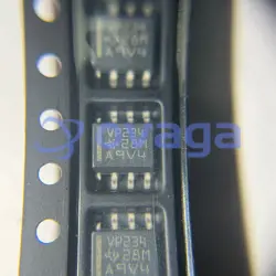
パッケージ/ケース: SOIC-8
RoHS ステータス:
在庫状況: 6884 個、新しいオリジナル
Warranty: 1 Year Ovaga Warranty - Find Out More
0
1
*すべての価格は米ドルです
| 数量 | 単価 | 外部価格 |
|---|---|---|
| 1 | $2.919 | $2.919 |
| 10 | $2.722 | $27.220 |
| 30 | $2.604 | $78.120 |
| 100 | $2.488 | $248.800 |
| 500 | $2.431 | $1215.500 |
| 1000 | $2.408 | $2408.000 |
In Stock:6884 PCS
SN65HVD1781QDRQ1 概要
These devices are designed to survive overvoltage faults such as direct shorts to power supplies, mis-wiring faults, connector failures, cable crushes, and tool mis-applications. They are also robust to ESD events, with high levels of protection to the human-body-model specification.
These devices combine a differential driver and a differential receiver, which operate from a single power supply. In the HVD1782, the driver differential outputs and the receiver differential inputs are connected internally to form a bus port suitable for half-duplex (two-wire bus) communication. This port features a wide common-mode voltage range, making the devices suitable for multipoint applications over long cable runs. These devices are characterized from –40°C to 125°C. These devices are pin-compatible with the industry-standard SN75176 transceiver, making them drop-in upgrades in most systems.
These devices are fully compliant with ANSI TIA/EIA 485-A with a 5-V supply and can operate with a 3.3-V supply with reduced driver output voltage for low-power applications. For applications where operation is required over an extended common-mode voltage range, see the SN65HVD1785 (SLLS872) data sheet.
特徴
- Qualified for Automotive Applications
- AEC-Q100 Qualified With the Following Results
- Device Temperature Grade 1:
–40°C to 125°C Ambient Operating Temperature Range - Device HBM ESD Classification Level H2
- Device CDM ESG Classification Level C3B
- Device Temperature Grade 1:
- Bus-Pin Fault Protection to:
- > ±70 V (’HVD1780-Q1, ’HVD1781-Q1)
- > ±30 V (’HVD1782-Q1)
- Operation With 3.3-V to 5-V Supply Range
- ±16-kV HBM Protection on Bus Pins
- Reduced Unit Load for up to 320 Nodes
- Failsafe Receiver for Open-Circuit, Short-Circuit and Idle-Bus Conditions
- Low Power Consumption
- Low Standby Supply Current, 1 µA Maximum
- ICC 4-mA Quiescent During Operation
- Pin-Compatible With Industry-Standard SN75176
- Signaling Rates of 115 kbps, 1 Mbps, and up to 10 Mbps
仕様
| パラメータ | 価値 | パラメータ | 価値 |
|---|---|---|---|
| Number of receivers | 1 | Number of transmitters | 1 |
| Duplex | Half | Supply voltage (nom) (V) | 3.3, 5 |
| Signaling rate (max) (MBits) | 1 | Fault protection (V) | -70 to 70 |
| Common-mode range (V) | -7 to 12 | Number of nodes | 320 |
| Features | Fault protection | Isolated | No |
| Supply current (max) (µA) | 6000 | Rating | Automotive |
| Operating temperature range (°C) | -40 to 125 |
配送
| 配送タイプ | 配送料 | リードタイム | |
|---|---|---|---|
 |
DHL | $20.00-$40.00 (0.50 KG) | 2-5 日々 |
 |
フェデックス | $20.00-$40.00 (0.50 KG) | 2-5 日々 |
 |
UPS | $20.00-$40.00 (0.50 KG) | 2-5 日々 |
 |
TNT | $20.00-$40.00 (0.50 KG) | 2-5 日々 |
 |
EMS | $20.00-$40.00 (0.50 KG) | 2-5 日々 |
 |
登録された航空便 | $20.00-$40.00 (0.50 KG) | 2-5 日々 |
処理時間:送料は地域や国によって異なります。
支払い
| 支払条件 | ハンドフィー | |
|---|---|---|
 |
電信送金 | 銀行手数料 US$30.00 を請求します。 |
 |
ペイパル | 4.0%のサービス料がかかります。 |
 |
クレジットカード | 3.5%のサービス料がかかります。 |
 |
ウエスタンユニオン | charge US.00 banking fee. |
 |
送金サービス | 銀行手数料は 0.00 米ドルかかります。 |
保証
1.購入した電子部品には365日保証が含まれており、製品の品質を保証します。
2.受け取った商品の一部が完璧な品質ではない場合、当社は責任を持って返金または交換を手配します。 ただし、商品は元の状態のままでなければなりません。
パッキング
-

ステップ1 :製品
-

ステップ2 :真空包装
-

ステップ3 :静電気防止袋
-

ステップ4 :個包装
-

ステップ5 :梱包箱
-

ステップ6 :バーコード配送タグ


すべての製品は静電気防止袋に梱包されます。 ESD 帯電防止保護を備えた状態で出荷されます。
社外の ESD 梱包ラベルには、部品番号、ブランド、数量などの当社の情報が使用されます。
私たちは出荷前にすべての商品を検査し、すべての製品が良好な状態であることを確認し、部品が新しいオリジナルでデータシートと一致していることを確認します。
すべての商品に問題がないことを確認した後、梱包後、安全に梱包し、グローバルエクスプレスで発送します。 優れた耐穿刺性と耐引裂性を示し、シールの完全性も良好です。


私たちは高品質の製品、思いやりのあるサービス、販売後の保証を提供します
-

豊富な商品を取り揃えておりますので、お客様の様々なニーズにお応え致します。
-

最小注文数量は1個からとなります。
-

最低国際配送料は0.00ドルから
-

全商品365日品質保証


