

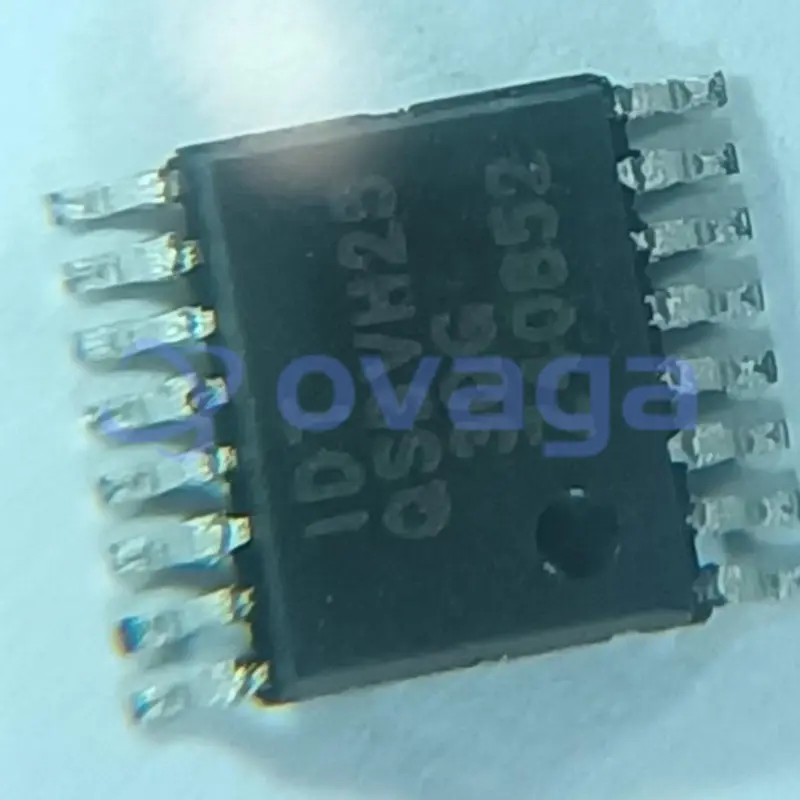
画像は参考用です。製品仕様を参照してください。
Renesas QS3VH253QG8
Encoders, Decoders, Multiplexers & Demultiplexers 3.3V Dual 1:4 Multi/ /Demultiplex


ブランド: Renesas Technology Corp
製造元部品 #: QS3VH253QG8
データシート: QS3VH253QG8 Datasheet (PDF)
パッケージ/ケース: TSOP20
製品の種類: ロジックIC
QS3VH253QG8 概要
The QS3VH253 HotSwitch Dual 4:1 multiplexer/demultiplexer is a high bandwidth bus switch with very low ON resistance, resulting in under 250ps propagation delay through the switch. The combination of near-zero propagation delay, high OFF impedance, and over-voltage tolerance makes the QS3VH253 ideal for high performance communication applications. The QS3VH253 operates from -40C to +85C.
特徴
- N channel FET switches with no parasitic diode to VCC
- Isolation under power-off conditions
- No DC path to VCC or GND
- 5V tolerant in OFF and ON state
- 5V tolerant I/Os
- Low RON - 4 ohm typical
- Flat RON characteristics over operating range
- Rail-to-rail switching 0 - 5V
- Bidirectional dataflow with near-zero delay: no added ground bounce
- Excellent RON matching between channels
- VCC operation: 2.3V to 3.6V
- High bandwidth - up to 500MHz
- LVTTL-compatible control Inputs
- Undershoot Clamp Diodes on all switch and control Inputs
- Low I/O capacitance, 4pF typical
- Available in 16 pin QSOP and TSSOP packages
仕様
| パラメータ | 価値 | パラメータ | 価値 |
|---|---|---|---|
| Pin Count | 16 | Package Category | Small Outline Packages |
| Released Date | Dec 11, 2017 |
配送
| 配送タイプ | 配送料 | リードタイム | |
|---|---|---|---|
 |
DHL | $20.00-$40.00 (0.50 KG) | 2-5 日々 |
 |
フェデックス | $20.00-$40.00 (0.50 KG) | 2-5 日々 |
 |
UPS | $20.00-$40.00 (0.50 KG) | 2-5 日々 |
 |
TNT | $20.00-$40.00 (0.50 KG) | 2-5 日々 |
 |
EMS | $20.00-$40.00 (0.50 KG) | 2-5 日々 |
 |
登録された航空便 | $20.00-$40.00 (0.50 KG) | 2-5 日々 |
処理時間:送料は地域や国によって異なります。
支払い
| 支払条件 | ハンドフィー | |
|---|---|---|
 |
電信送金 | 銀行手数料 US$30.00 を請求します。 |
 |
ペイパル | 4.0%のサービス料がかかります。 |
 |
クレジットカード | 3.5%のサービス料がかかります。 |
 |
ウエスタンユニオン | charge US.00 banking fee. |
 |
送金サービス | 銀行手数料は 0.00 米ドルかかります。 |
保証
1.購入した電子部品には365日保証が含まれており、製品の品質を保証します。
2.受け取った商品の一部が完璧な品質ではない場合、当社は責任を持って返金または交換を手配します。 ただし、商品は元の状態のままでなければなりません。
パッキング
-

ステップ1 :製品
-

ステップ2 :真空包装
-

ステップ3 :静電気防止袋
-

ステップ4 :個包装
-

ステップ5 :梱包箱
-

ステップ6 :バーコード配送タグ


すべての製品は静電気防止袋に梱包されます。 ESD 帯電防止保護を備えた状態で出荷されます。
社外の ESD 梱包ラベルには、部品番号、ブランド、数量などの当社の情報が使用されます。
私たちは出荷前にすべての商品を検査し、すべての製品が良好な状態であることを確認し、部品が新しいオリジナルでデータシートと一致していることを確認します。
すべての商品に問題がないことを確認した後、梱包後、安全に梱包し、グローバルエクスプレスで発送します。 優れた耐穿刺性と耐引裂性を示し、シールの完全性も良好です。


パーツポイント
-
The QS3VH253QG8 chip is an advanced semiconductor device that serves as a high-speed reversible multiplexer/demultiplexer. It offers a low ON resistance and wide voltage range, allowing for efficient data transfer between multiple sources. The chip is commonly used in digital signal processing applications and can handle high-speed data rates, making it a valuable component in various electronic systems.
-
Equivalent
There are no direct equivalent products to the QS3VH253QG8 chip. However, potential alternatives may include similar voltage-controlled switches or multiplexers from other manufacturers such as Texas Instruments, Maxim Integrated, or NXP Semiconductors. A detailed search of these manufacturers' catalogs may provide suitable alternatives for specific applications. -
Features
The QS3VH253QG8 is a 32-channel video switch with a dual 2:1 multiplexer and an output enable function. It offers high-speed switching with low switch capacitance and charges and low power consumption. It operates on a voltage range of 3.0V to 3.6V and is compatible with various interface standards. -
Pinout
The QS3VH253QG8 is a 16-pin quad 2:1 multiplexer/demultiplexer with 3-state outputs. It is used for signal routing and selection in digital circuits, allowing one of two input signals to be selected and routed to the output. Its 3-state outputs allow for high impedance when not in use. -
Manufacturer
QS3VH253QG8 is a product made by ON Semiconductor. ON Semiconductor is a global supplier of semiconductor-based solutions, specializing in power and energy-efficient systems. The company designs, manufactures, and sells a wide range of semiconductors to various industries, including automotive, industrial, consumer electronics, and more. -
Application Field
The application areas of the QS3VH253QG8 include various electronic devices and systems where high-speed data transmission, signal isolation, and voltage translation are required. This can include applications in data communication, networking equipment, test and measurement instruments, industrial automation, and any other applications that necessitate reliable and efficient signal switching and routing. -
Package
The QS3VH253QG8 chip is available in a QSOP package type, designed in a quad flat no-lead form. It has a fairly small size, typically measuring around 5mm x 7mm.


データシート PDF
私たちは高品質の製品、思いやりのあるサービス、販売後の保証を提供します
-

豊富な商品を取り揃えておりますので、お客様の様々なニーズにお応え致します。
-

最小注文数量は1個からとなります。
-

最低国際配送料は0.00ドルから
-

全商品365日品質保証


I am extremely satisfied with the electronic components I purchased from Ovaga.