

画像は参考用です。製品仕様を参照してください。
注文金額が
$5000
Xilinx XC7K160T-2FFG676C

FPGA - Field Programmable Gate Array XC7K160T-2FFG676C


ブランド: AMD Xilinx, Inc
製造元部品 #: XC7K160T-2FFG676C
データシート: XC7K160T-2FFG676C Datasheet (PDF)
パッケージ/ケース: KINTEX-7
RoHS ステータス:
在庫状況: 3,002 個、新しいオリジナル
製品の種類: FPGAs (Field Programmable Gate Array)
Warranty: 1 Year Ovaga Warranty - Find Out More
0
1
*すべての価格は米ドルです
| 数量 | 単価 | 外部価格 |
|---|---|---|
| 1 | $58.079 | $58.079 |
| 3 | $53.202 | $159.606 |
| 40 | $50.985 | $2039.400 |
在庫あり: 3,002 PCS
XC7K160T-2FFG676C 概要
The XC7K160T-2FFG676C is a field-programmable gate array (FPGA) from Xilinx, belonging to the Kintex-7 family.
特徴
Family: Kintex-7 is a family of FPGAs by Xilinx, known for a balance of performance, power efficiency, and cost-effectiveness.
Logic Cells: The "160T" in the part number indicates that this FPGA has approximately 160,000 logic cells. Logic cells are the basic building blocks of programmable logic within the FPGA.
Package Type: The "FFG676" indicates the package type. "FFG" stands for Fine-pitch Ball Grid Array, and "676" indicates the number of pins on the package.
Speed Grade: The "-2" in the part number denotes the speed grade. Different speed grades offer variations in terms of maximum operating frequency.
Configuration: Being a field-programmable device, the configuration is stored in external memory (e.g., Flash) and loaded into the FPGA upon power-up.
I/Os (Input/Output): The number and type of I/O pins can vary between FPGA models. In this case, "676" in the package type suggests 676 pins are available for I/O.
Block RAM: Kintex-7 FPGAs include embedded block RAM (BRAM) for data storage.
DSP Slices: Digital Signal Processing (DSP) slices are hardware blocks specialized for mathematical operations. The specific number of DSP slices can vary between FPGA models.
PCI Express: Some FPGAs in the Kintex-7 family support PCI Express (PCIe) interfaces for high-speed communication.
Clock Management: Integrated clock management resources allow for efficient clock distribution and control within the FPGA.
応用
FPGAs like the Kintex-7 series are used in a variety of applications, including telecommunications, networking, industrial automation, and signal processing.

配送
| 配送タイプ | 配送料 | リードタイム | |
|---|---|---|---|
 |
DHL | $20.00-$40.00 (0.50 KG) | 2-5 日々 |
 |
フェデックス | $20.00-$40.00 (0.50 KG) | 2-5 日々 |
 |
UPS | $20.00-$40.00 (0.50 KG) | 2-5 日々 |
 |
TNT | $20.00-$40.00 (0.50 KG) | 2-5 日々 |
 |
EMS | $20.00-$40.00 (0.50 KG) | 2-5 日々 |
 |
登録された航空便 | $20.00-$40.00 (0.50 KG) | 2-5 日々 |
処理時間:送料は地域や国によって異なります。
支払い
| 支払条件 | ハンドフィー | |
|---|---|---|
 |
電信送金 | 銀行手数料 US$30.00 を請求します。 |
 |
ペイパル | 4.0%のサービス料がかかります。 |
 |
クレジットカード | 3.5%のサービス料がかかります。 |
 |
ウエスタンユニオン | charge US.00 banking fee. |
 |
送金サービス | 銀行手数料は 0.00 米ドルかかります。 |
保証
1.購入した電子部品には365日保証が含まれており、製品の品質を保証します。
2.受け取った商品の一部が完璧な品質ではない場合、当社は責任を持って返金または交換を手配します。 ただし、商品は元の状態のままでなければなりません。
パッキング
-

ステップ1 :製品
-

ステップ2 :真空包装
-

ステップ3 :静電気防止袋
-

ステップ4 :個包装
-

ステップ5 :梱包箱
-

ステップ6 :バーコード配送タグ


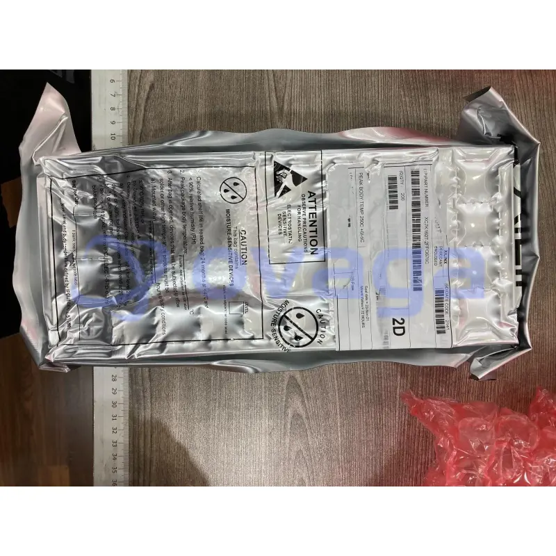
すべての製品は静電気防止袋に梱包されます。 ESD 帯電防止保護を備えた状態で出荷されます。
社外の ESD 梱包ラベルには、部品番号、ブランド、数量などの当社の情報が使用されます。
私たちは出荷前にすべての商品を検査し、すべての製品が良好な状態であることを確認し、部品が新しいオリジナルでデータシートと一致していることを確認します。
すべての商品に問題がないことを確認した後、梱包後、安全に梱包し、グローバルエクスプレスで発送します。 優れた耐穿刺性と耐引裂性を示し、シールの完全性も良好です。


データシート PDF
私たちは高品質の製品、思いやりのあるサービス、販売後の保証を提供します
-

豊富な商品を取り揃えておりますので、お客様の様々なニーズにお応え致します。
-

最小注文数量は1個からとなります。
-

最低国際配送料は0.00ドルから
-

全商品365日品質保証


