

画像は参考用です。製品仕様を参照してください。
注文金額が
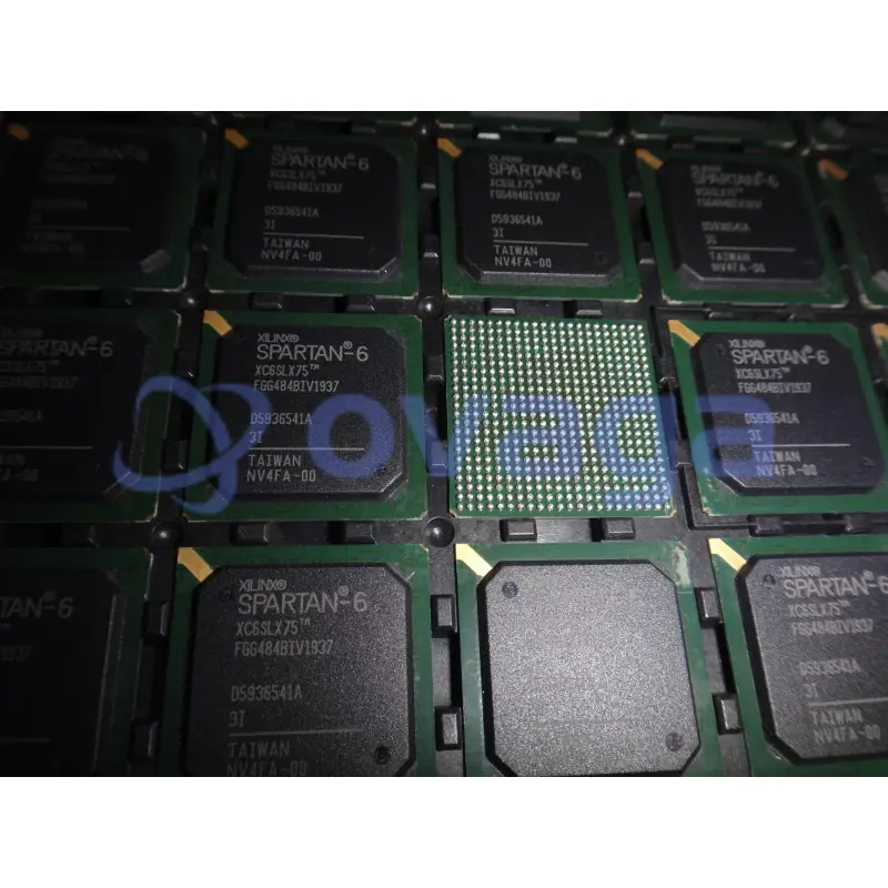
$5000Xilinx XC6SLX75-3FGG484I
XC6SLX75-3FGG484I FPGA Field Programmable Gate Array


ブランド: AMD Xilinx, Inc
製造元部品 #: XC6SLX75-3FGG484I
データシート: XC6SLX75-3FGG484I Datasheet (PDF)
パッケージ/ケース: BGA-484
XC6SLX75-3FGG484I 概要
Xilinx's XC6SLX75-3FGG484I FPGA is a versatile and cost-effective solution that excels in performance, energy efficiency, and design flexibility. Belonging to the Spartan-6 family, this FPGA is highly regarded for its ability to deliver robust performance while consuming minimal power. The "LX" designation underscores its low power characteristics, making it an ideal choice for projects that prioritize energy efficiency. With a logic capacity of approximately 75,000 cells, the XC6SLX75-3FGG484I offers a wealth of resources for implementing custom logic tailored to specific requirements. Operating at a maximum core voltage of 3.3 volts ("-3"), this FPGA ensures reliable operation across a range of applications. The FGG484I package type, featuring 484 pins in a Fine-Pitch Ball Grid Array (FBGA) configuration, enables convenient surface-mount installation and seamless connectivity to external circuitry

仕様
| パラメータ | 価値 | パラメータ | 価値 |
|---|---|---|---|
| Manufacturer: | Xilinx | Product Category: | FPGA - Field Programmable Gate Array |
| RoHS: | Y | Product: | Spartan-6 |
| Number of Logic Elements: | 74637 | Number of I/Os: | 280 I/O |
| Operating Supply Voltage: | 1.2 V | Minimum Operating Temperature: | - 40 C |
| Maximum Operating Temperature: | + 100 C | Mounting Style: | SMD/SMT |
| Package / Case: | FCBGA-484 | Series: | XC6SLX75 |
| Brand: | Xilinx | Distributed RAM: | 692 kbit |
| Embedded Block RAM - EBR: | 3096 kbit | Maximum Operating Frequency: | 1080 MHz |
| Moisture Sensitive: | Yes | Product Type: | FPGA - Field Programmable Gate Array |
| Factory Pack Quantity: | 60 | Subcategory: | Programmable Logic ICs |
| Tradename: | Spartan | Tags | XC6SLX75-3FGG, XC6SLX75-3F, XC6SLX75-3, XC6SLX7, XC6SLX, XC6SL, XC6S, XC6 |
| Adaptive Logic Modules - ALMs: | 11662 ALM | Embedded Memory: | 3.02 Mbit |
| Supply Voltage - Min: | 1.14 V | Supply Voltage - Max: | 1.26 V |
| Data Rate: | - | Number of Transceivers: | - |
| Number of Logic Array Blocks - LABs: | 5831 LAB |
配送
| 配送タイプ | 配送料 | リードタイム | |
|---|---|---|---|
 |
DHL | $20.00-$40.00 (0.50 KG) | 2-5 日々 |
 |
フェデックス | $20.00-$40.00 (0.50 KG) | 2-5 日々 |
 |
UPS | $20.00-$40.00 (0.50 KG) | 2-5 日々 |
 |
TNT | $20.00-$40.00 (0.50 KG) | 2-5 日々 |
 |
EMS | $20.00-$40.00 (0.50 KG) | 2-5 日々 |
 |
登録された航空便 | $20.00-$40.00 (0.50 KG) | 2-5 日々 |
処理時間:送料は地域や国によって異なります。
支払い
| 支払条件 | ハンドフィー | |
|---|---|---|
 |
電信送金 | 銀行手数料 US$30.00 を請求します。 |
 |
ペイパル | 4.0%のサービス料がかかります。 |
 |
クレジットカード | 3.5%のサービス料がかかります。 |
 |
ウエスタンユニオン | charge US.00 banking fee. |
 |
送金サービス | 銀行手数料は 0.00 米ドルかかります。 |
保証
1.購入した電子部品には365日保証が含まれており、製品の品質を保証します。
2.受け取った商品の一部が完璧な品質ではない場合、当社は責任を持って返金または交換を手配します。 ただし、商品は元の状態のままでなければなりません。
パッキング
-

ステップ1 :製品
-

ステップ2 :真空包装
-

ステップ3 :静電気防止袋
-

ステップ4 :個包装
-

ステップ5 :梱包箱
-

ステップ6 :バーコード配送タグ


すべての製品は静電気防止袋に梱包されます。 ESD 帯電防止保護を備えた状態で出荷されます。
社外の ESD 梱包ラベルには、部品番号、ブランド、数量などの当社の情報が使用されます。
私たちは出荷前にすべての商品を検査し、すべての製品が良好な状態であることを確認し、部品が新しいオリジナルでデータシートと一致していることを確認します。
すべての商品に問題がないことを確認した後、梱包後、安全に梱包し、グローバルエクスプレスで発送します。 優れた耐穿刺性と耐引裂性を示し、シールの完全性も良好です。


パーツポイント
-
The XC6SLX75-3FGG484I chip is a field-programmable gate array (FPGA) manufactured by Xilinx. It has 75,840 logic cells and offers a range of features including high-performance connectivity, automated performance analysis, and multi-gigabit serial I/O capabilities. The chip's FG484 package type indicates a fine-pitch ball grid array with 484 pins, suitable for use in various applications including telecommunications, automotive, and industrial sectors.
-
Features
The XC6SLX75-3FGG484I is a Field Programmable Gate Array (FPGA) designed by Xilinx. It has a total of 75,360 logic cells, 1,920 Kbits of block RAM, and 560 DSP slices. It operates at a maximum clock frequency of 300 MHz and uses the FG484 package. It supports various communication protocols and offers advanced features for digital logic design. -
Pinout
The XC6SLX75-3FGG484I is a field-programmable gate array (FPGA) with a pin count of 484. It is designed by Xilinx and has a 75,000 logic cell count. The specific functions of each pin can be found in the datasheet of the device. -
Manufacturer
The manufacturer of the XC6SLX75-3FGG484I is Xilinx Inc. Xilinx is a prominent American technology company specializing in the development and manufacturing of programmable logic devices and related software tools. They are known for their field-programmable gate arrays (FPGA), which are integrated circuits that can be customized to execute specific functions as per user requirements. -
Application Field
The XC6SLX75-3FGG484I is a field-programmable gate array (FPGA) that can be used in various application areas, including wireless communication, industrial automation, video and image processing, and automotive applications. Its high-performance logic fabric and low power consumption make it suitable for a range of digital signal processing and control tasks. -
Package
The XC6SLX75-3FGG484I chip is offered in a 484-pin Fine-Pitch Ball Grid Array (FBGA) package type. The package form is Grid Array, and its size is 23mm x 23mm.


データシート PDF
私たちは高品質の製品、思いやりのあるサービス、販売後の保証を提供します
-

豊富な商品を取り揃えておりますので、お客様の様々なニーズにお応え致します。
-

最小注文数量は1個からとなります。
-

最低国際配送料は0.00ドルから
-

全商品365日品質保証


