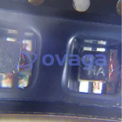
画像は参考用です。製品仕様を参照してください。
注文金額が
$5000
LCMXO1200C-3FTN256C

Versatile FPGA solution with 1200 Logic Units and 211 Input/Output ports


ブランド: Lattice Semiconductor Corporation
製造元部品 #: LCMXO1200C-3FTN256C
データシート: LCMXO1200C-3FTN256C データシート (PDF)
パッケージ/ケース: 256-LBGA
RoHS ステータス:
在庫状況: 7,384 個、新しいオリジナル
製品の種類: FPGAs (Field Programmable Gate Array)
Warranty: 1 Year Ovaga Warranty - Find Out More
0
1
*すべての価格は米ドルです
| 数量 | 単価 | 外部価格 |
|---|---|---|
| 1 | $24.004 | $24.004 |
| 200 | $9.289 | $1857.800 |
| 500 | $8.963 | $4481.500 |
| 1000 | $8.801 | $8801.000 |
在庫あり: 7,384 PCS
LCMXO1200C-3FTN256C 概要
The LCMXO1200C-3FTN256C FPGA from Lattice Semiconductor is a powerful yet cost-effective solution for a wide range of applications. With its 1200 LUTs, 64 Kbit Embedded Block RAM, and 18 I/O pins, this FPGA offers the flexibility and performance needed for industrial control systems, consumer electronics, automotive infotainment, and communication equipment. Its low power consumption and compact 256-pin TQFP package make it a great choice for space-constrained designs, while its maximum frequency of 75 MHz ensures efficient operation
特徴
- Non-volatile, Infinitely Reconfigurable
- Instant-on – powers up in microseconds
- Single chip, no external configuration memory
- required
- Excellent design security, no bit stream to
- intercept
- Reconfigure SRAM based logic in milliseconds
- SRAM and non-volatile memory programmable
- through JTAG port
- Supports background programming of
- non-volatile memory
- Sleep Mode
- Allows up to 100x static current reduction
- TransFR™ Reconfiguration (TFR)
- In-field logic update while system operates
- High I/O to Logic Density
- 256 to 2280 LUT4s
- 73 to 271 I/Os with extensive package options
- Density migration supported
- Lead free/RoHS compliant packaging
- Embedded and Distributed Memory
- Up to 27.6 Kbits sysMEM™ Embedded Block
- RAM
- Up to 7.5 Kbits distributed RAM
- Dedicated FIFO control logic
- Flexible I/O Buffer
- Programmable sysIO™ buffer supports wide
- range of interfaces:
- − LVCMOS 3.3/2.5/1.8/1.5/1.2
- − LVTTL
- − PCI
- − LVDS, Bus-LVDS, LVPECL, RSDS
- sysCLOCK™ PLLs
- Up to two analog PLLs per device
- Clock multiply, divide, and phase shifting
- System Level Support
- IEEE Standard 1149.1 Boundary Scan
- Onboard oscillator
- Devices operate with 3.3V, 2.5V, 1.8V or 1.2V
- power supply
- IEEE 1532 compliant in-system programming
仕様
| パラメータ | 価値 | パラメータ | 価値 |
|---|---|---|---|
| Series | MachXO | Package | Tray |
| Product Status | Active | Programmabe | Not Verified |
| Number of LABs/CLBs | 150 | Number of Logic Elements/Cells | 1200 |
| Total RAM Bits | 9421 | Number of I/O | 211 |
| Voltage - Supply | 1.71V ~ 3.465V | Mounting Type | Surface Mount |
| Operating Temperature | 0°C ~ 85°C (TJ) | Package / Case | 256-LBGA |
| Supplier Device Package | 256-FTBGA (17x17) |
配送
| 配送タイプ | 配送料 | リードタイム | |
|---|---|---|---|
 |
DHL | $20.00-$40.00 (0.50 KG) | 2-5 日々 |
 |
フェデックス | $20.00-$40.00 (0.50 KG) | 2-5 日々 |
 |
UPS | $20.00-$40.00 (0.50 KG) | 2-5 日々 |
 |
TNT | $20.00-$40.00 (0.50 KG) | 2-5 日々 |
 |
EMS | $20.00-$40.00 (0.50 KG) | 2-5 日々 |
 |
登録された航空便 | $20.00-$40.00 (0.50 KG) | 2-5 日々 |
処理時間:送料は地域や国によって異なります。
支払い
| 支払条件 | ハンドフィー | |
|---|---|---|
 |
電信送金 | 銀行手数料 US$30.00 を請求します。 |
 |
ペイパル | 4.0%のサービス料がかかります。 |
 |
クレジットカード | 3.5%のサービス料がかかります。 |
 |
ウエスタンユニオン | charge US.00 banking fee. |
 |
送金サービス | 銀行手数料は 0.00 米ドルかかります。 |
保証
1.購入した電子部品には365日保証が含まれており、製品の品質を保証します。
2.受け取った商品の一部が完璧な品質ではない場合、当社は責任を持って返金または交換を手配します。 ただし、商品は元の状態のままでなければなりません。
パッキング
-

ステップ1 :製品
-

ステップ2 :真空包装
-

ステップ3 :静電気防止袋
-

ステップ4 :個包装
-

ステップ5 :梱包箱
-

ステップ6 :バーコード配送タグ


すべての製品は静電気防止袋に梱包されます。 ESD 帯電防止保護を備えた状態で出荷されます。
社外の ESD 梱包ラベルには、部品番号、ブランド、数量などの当社の情報が使用されます。
私たちは出荷前にすべての商品を検査し、すべての製品が良好な状態であることを確認し、部品が新しいオリジナルでデータシートと一致していることを確認します。
すべての商品に問題がないことを確認した後、梱包後、安全に梱包し、グローバルエクスプレスで発送します。 優れた耐穿刺性と耐引裂性を示し、シールの完全性も良好です。


パーツポイント
-
LCMXO1200C-3FTN256C is a low-power, small form-factor FPGA chip from Lattice Semiconductor. It features 1200 LUTs, 64Kb embedded block RAM, and dedicated FPGA fabric for low-power applications. The chip is designed for applications requiring high performance and low power consumption in a compact package.
-
Equivalent
Some equivalent products of LCMXO1200C-3FTN256C chip are LCMXO1200C-3FTN256C-ND, LCMXO1200C-3FTN256C-TR, and LCMXO1200C-3FTN256C-WS. These chips are all in the Lattice XO2-1200 family, offering similar features and functionality. -
Features
LCMXO1200C-3FTN256C is a low-power, cost-effective FPGA with 1200 Look-Up Tables (LUTs), 64Kb Embedded Block RAM, 65 I/Os, and 4 multipliers. It operates at 3.3V and offers non-volatile configuration memory, instant-on capability, and high security with AES bitstream encryption. -
Pinout
The LCMXO1200C-3FTN256C is a field programmable gate array (FPGA) with 256 pins in a 256-pin fine-pitch BGA package. It features a high density of logic elements and embedded block RAM, making it suitable for a wide range of applications in the consumer, communications, and industrial markets. -
Manufacturer
Lattice Semiconductor is the manufacturer of the LCMXO1200C-3FTN256C. Lattice Semiconductor is an American company that specializes in programmable logic devices and related software, offering a wide range of solutions for the communications, computing, industrial, automotive, and consumer markets. -
Application Field
The LCMXO1200C-3FTN256C is commonly used in applications such as portable medical devices, handheld instruments, industrial control systems, and test & measurement equipment. Its low power consumption, small form factor, and high integration make it well-suited for applications requiring programmable logic with low power requirements and limited space. -
Package
The LCMXO1200C-3FTN256C chip is in a surface mount package, in the form of a BGA (Ball Grid Array) and is 13mm x 13mm in size.


私たちは高品質の製品、思いやりのあるサービス、販売後の保証を提供します
-

豊富な商品を取り揃えておりますので、お客様の様々なニーズにお応え致します。
-

最小注文数量は1個からとなります。
-

最低国際配送料は0.00ドルから
-

全商品365日品質保証