


画像は参考用です。製品仕様を参照してください。
注文金額が
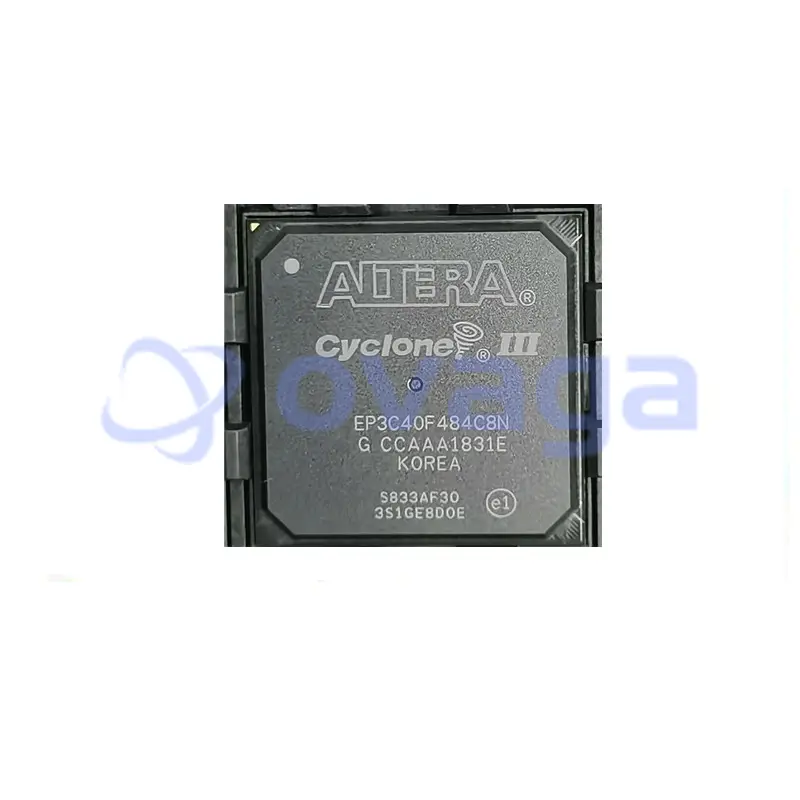
$5000Altera EP3C40F484C8N
With its advanced architecture and high-speed I/O interfaces


ブランド: Altera Corporation (Intel)
製造元部品 #: EP3C40F484C8N
データシート: EP3C40F484C8N Datasheet (PDF)
パッケージ/ケース: FBGA-484
EP3C40F484C8N 概要
The EP3C40F484C8N is a versatile solution for a wide range of applications, including telecommunications, industrial automation, and embedded systems. Its surface mount device termination type simplifies the assembly process, while the FPGA's scalability and flexibility make it a cost-effective choice for prototype development and volume production
特徴
- It contains 39,600 logic elements (LEs) and 1,260 embedded memory blocks (MBs).
- It has a maximum of 550 user I/O pins.
- It operates at a maximum frequency of 400 MHz.
- It has various configurable features such as PLLs (Phase-Locked Loops), memory controllers, and transceivers.
応用
- Industrial automation
- Video and image processing
- Network processing
- Medical equipment
- Aerospace and defense systems
- Automotive systems
仕様
| パラメータ | 価値 | パラメータ | 価値 |
|---|---|---|---|
| feature-family-name | Cyclone® III | feature-process-technology | 65nm |
| feature-maximum-number-of-user-i-os | 331 | feature-number-of-registers | |
| feature-device-logic-cells | 39600 | feature-device-system-gates | |
| feature-number-of-multipliers | 126 (18x18) | feature-program-memory-type | SRAM |
| feature-ram-bits-kbit | 1134 | feature-total-number-of-block-ram | 126 |
| feature-ethernet-macs | feature-supported-ip-core | Viterbi Compiler, Low-Speed/Hybrid Serial Decoder|V1 ColdFire|SpeedView Enabled JPEG Encoder (SVE-JPEG-E)|10 Gigabit Ethernet MAC|32/64-bit PCI-X bus Master/Target interface Core, 66/100/133Mhz | |
| feature-supported-ip-core-manufacture | Altera/Freescale/CAST, Inc/MorethanIP/PLDA | feature-maximum-number-of-serdes-channels | |
| feature-device-logic-units | 39600 | feature-device-number-of-dlls-plls | 4 |
| feature-transceiver-blocks | feature-transceiver-speed-gbps | ||
| feature-dedicated-dsp | feature-pci-blocks | ||
| feature-programmability | No | feature-maximum-internal-frequency-mhz | 402 |
| feature-speed-grade | 8 | feature-giga-multiply-accumulates-per-second | |
| feature-differential-i-o-standards-supported | LVPECL|LVDS|HSTL-18|HSTL-15|HSTL-12|SSTL-2|SSTL-18|RSDS | feature-single-ended-i-o-standards-supported | LVTTL|LVCMOS|PCI|PCI-X|SSTL|HSTL |
| feature-external-memory-interface | DDR2 SDRAM|QDRII+SRAM | feature-minimum-operating-supply-voltage-v | 1.15 |
| feature-maximum-operating-supply-voltage-v | 1.25 | feature-packaging | Tray |
| feature-rohs | feature-rad-hard | ||
| feature-pin-count | 484 | feature-supplier-package | FBGA |
| feature-standard-package-name1 | BGA | feature-cecc-qualified | No |
| feature-esd-protection | feature-escc-qualified | ||
| feature-military | No | feature-aec-qualified | No |
| feature-aec-qualified-number | feature-auto-motive | No | |
| feature-p-pap | No | feature-eccn-code | 3A991 |
| feature-svhc | No |
配送
| 配送タイプ | 配送料 | リードタイム | |
|---|---|---|---|
 |
DHL | $20.00-$40.00 (0.50 KG) | 2-5 日々 |
 |
フェデックス | $20.00-$40.00 (0.50 KG) | 2-5 日々 |
 |
UPS | $20.00-$40.00 (0.50 KG) | 2-5 日々 |
 |
TNT | $20.00-$40.00 (0.50 KG) | 2-5 日々 |
 |
EMS | $20.00-$40.00 (0.50 KG) | 2-5 日々 |
 |
登録された航空便 | $20.00-$40.00 (0.50 KG) | 2-5 日々 |
処理時間:送料は地域や国によって異なります。
支払い
| 支払条件 | ハンドフィー | |
|---|---|---|
 |
電信送金 | 銀行手数料 US$30.00 を請求します。 |
 |
ペイパル | 4.0%のサービス料がかかります。 |
 |
クレジットカード | 3.5%のサービス料がかかります。 |
 |
ウエスタンユニオン | charge US.00 banking fee. |
 |
送金サービス | 銀行手数料は 0.00 米ドルかかります。 |
保証
1.購入した電子部品には365日保証が含まれており、製品の品質を保証します。
2.受け取った商品の一部が完璧な品質ではない場合、当社は責任を持って返金または交換を手配します。 ただし、商品は元の状態のままでなければなりません。
パッキング
-

ステップ1 :製品
-

ステップ2 :真空包装
-

ステップ3 :静電気防止袋
-

ステップ4 :個包装
-

ステップ5 :梱包箱
-

ステップ6 :バーコード配送タグ


すべての製品は静電気防止袋に梱包されます。 ESD 帯電防止保護を備えた状態で出荷されます。
社外の ESD 梱包ラベルには、部品番号、ブランド、数量などの当社の情報が使用されます。
私たちは出荷前にすべての商品を検査し、すべての製品が良好な状態であることを確認し、部品が新しいオリジナルでデータシートと一致していることを確認します。
すべての商品に問題がないことを確認した後、梱包後、安全に梱包し、グローバルエクスプレスで発送します。 優れた耐穿刺性と耐引裂性を示し、シールの完全性も良好です。


同等部品
のために EP3C40F484C8N コンポーネントの場合は、これらの交換部品および代替部品を検討してください:
部品番号
ブランド
パッケージ
説明
パーツポイント
-
EP3C40F484C8N is a programmable chip developed by Altera. It belongs to the Cyclone III FPGA family and is designed for a broad range of applications. With 40,000 logic elements, 583 I/O pins, and various high-speed interfaces, it offers high performance and flexibility. The C8N package refers to the chip's 484-pin FineLine BGA package. Overall, EP3C40F484C8N is ideal for complex digital systems and offers customization options through its programmable logic.
-
Equivalent
Equivalent products of the EP3C40F484C8N chip include EP3C40F484I8N, EP3C40F484I7N, EP3C40F484I8LN, and EP3C40F484I7LN from the same Cyclone III FPGA family by Altera/Intel. -
Features
EP3C40F484C8N is a Cyclone III FPGA (Field-Programmable Gate Array) with 40,020 logic elements, 1,134 Kbits RAM, and 346 multiplexers. It operates at a maximum clock frequency of 408 MHz and has 249 user I/O pins. This FPGA offers high performance, low power consumption, and is suited for a wide range of applications. -
Pinout
The EP3C40F484C8N is an FPGA with a pin count of 484. Its function is to program and configure digital logic circuits to perform specific tasks. The FPGA can be customized to meet specific requirements and is often used in applications such as telecommunications, image and video processing, and embedded systems. -
Manufacturer
EP3C40F484C8N is manufactured by Altera, which is a company specializing in the production of programmable logic devices and associated software and development tools. Altera, now a part of Intel Corporation, offers a range of FPGA (field-programmable gate array) solutions for various applications in sectors like automotive, telecommunications, industrial automation, and more. -
Application Field
The EP3C40F484C8N is a field-programmable gate array (FPGA) that is commonly used in various applications such as automotive systems, industrial automation, communication systems, and image and video processing. Its high-performance and flexible architecture make it suitable for a wide range of electronic design projects. -
Package
The EP3C40F484C8N chip is offered in a standard plastic package of FBGA (Fine-pitch Ball Grid Array) type. It has 484 contacts and its form, or physical dimensions, are designed for a small footprint, making it suitable for various applications.


データシート PDF
私たちは高品質の製品、思いやりのあるサービス、販売後の保証を提供します
-

豊富な商品を取り揃えておりますので、お客様の様々なニーズにお応え致します。
-

最小注文数量は1個からとなります。
-

最低国際配送料は0.00ドルから
-

全商品365日品質保証


