

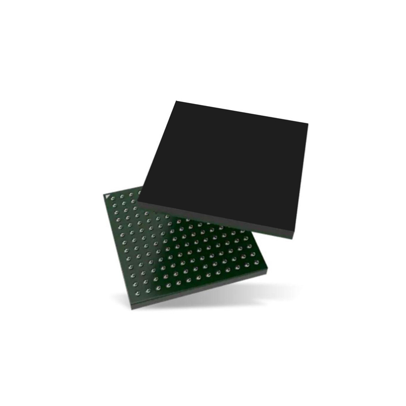
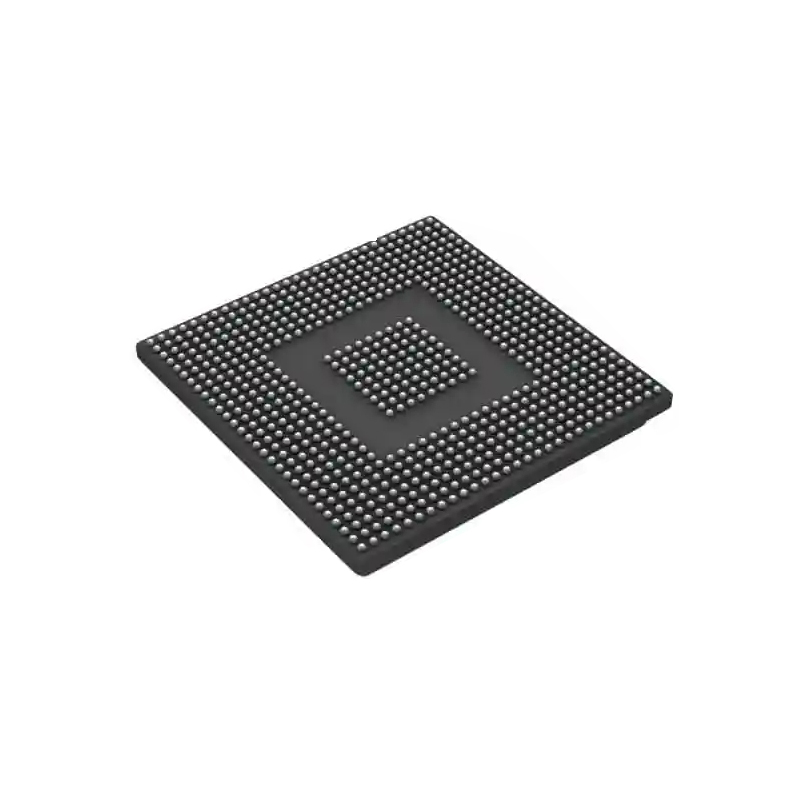
画像は参考用です。製品仕様を参照してください。
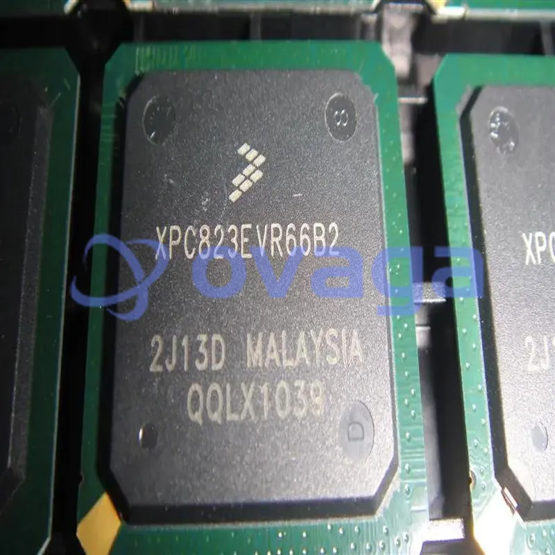
NXP XPC823EVR66B2
Microprocessors - MPU PB-FREE 823E 66MHZ


ブランド: NXP
製造元部品 #: XPC823EVR66B2
データシート: XPC823EVR66B2 データシート (PDF)
パッケージ/ケース: PBGA-256
製品の種類: Microprocessors - MPU
XPC823EVR66B2 概要
PowerPC Microprocessor IC MPC8xx 1 Core, 32-Bit 66MHz 256-PBGA (23x23)
特徴
- The following list summarizes the key MPC860
- features:
- Embedded single-issue, 32-bit MPC8xx core (implementing the PowerPC architecture) with thirty-two 32-bit general-purpose registers (GPRs)
- — The core performs branch prediction with conditional prefetch, without conditional execution
- — 4- or 8-Kbyte data cache and 4- or 16-Kbyte instruction cache (see Table 1)
- – 16-Kbyte instruction caches are four-way, set-associative with 256 sets;
- 4-Kbyte instruction caches are two-way, set-associative with 128 sets.
- – 8-Kbyte data caches are two-way, set-associative with 256 sets; 4-Kbyte data caches are two-way, set-associative with 128 sets.
- – Cache coherency for both instruction and data caches is maintained on 128-bit (4-word) cache blocks.
- – Caches are physically addressed, implement a least recently used (LRU) replacement algorithm, and are lockable on a cache block basis.
- — Instruction and data caches are two-way, set-associative, physically addressed, LRU replacement, and lockable on-line granularity.
- — MMUs with 32-entry TLB, fully associative instruction, and data TLBs
- — MMUs support multiple page sizes of 4, 16, and 512 Kbytes, and 8 Mbytes; 16 virtual address spaces and 16 protection groups
- — Advanced on-chip-emulation debug mode
- Up to 32-bit data bus (dynamic bus sizing for 8, 16, and 32 bits)
- 32 address lines
- Operates at up to 80 MHz
- Memory controller (eight banks)
- — Contains complete dynamic RAM (DRAM) controller
- — Each bank can be a chip select or RASto support a DRAM bank
- — Up to 15 wait states programmable per memory bank
- — Glueless interface to DRAM, SIMMS, SRAM, EPROM, Flash EPROM, and other memory devices.
- — DRAM controller programmable to support most size and speed memory interfaces
- — Four CASlines, four WElines, one OEline
- — Boot chip-select available at reset (options for 8-, 16-, or 32-bit memory)
- — Variable block sizes (32 Kbyte to 256 Mbyte)
- — Selectable write protection
- — On-chip bus arbitration logic
- General-purpose timers
- — Four 16-bit timers or two 32-bit timers
- — Gate mode can enable/disable counting
- — Interrupt can be masked on reference match and event capture
- System integration unit (SIU)
- — Bus monitor
- — Software watchdog
- — Periodic interrupt timer (PIT)
- — Low-power stop mode
- — Clock synthesizer
- — Three parallel I/O registers with open-drain capability
- Four baud-rate generators (BRGs)
- — Independent (can be connected to any SCC or SMC)
- — Allow changes during operation
- — Autobaud support option
- Four serial communications controllers (SCCs)
- — Ethernet/IEEE 802.3 optional on SCC1–4, supporting full 10-Mbps operation (available only on specially programmed devices).
- — HDLC/SDLC(all channels supported at 2 Mbps)
- — HDLC bus (implements an HDLC-based local area network (LAN))
- — Asynchronous HDLC to support PPP (point-to-point protocol)
- — AppleTalk
- — Universal asynchronous receiver transmitter (UART)
- — Synchronous UART
- — Serial infrared (IrDA)
- — Binary synchronous communication (BISYNC)
- — Totally transparent (bit streams)
- — Totally transparent (frame based with optional cyclic redundancy check (CRC))
- Two SMCs (serial management channels)
- — UART
- — Transparent
- — General circuit interface (GCI) controller
- — Can be connected to the time-division multiplexed (TDM) channels
- One SPI (serial peripheral interface)
- — Supports master and slave modes
- — Supports multimaster operation on the same bus
- One I2C (inter-integrated circuit) port
- — Supports master and slave modes
- — Multiple-master environment support
- Time-slot assigner (TSA)
- — Allows SCCs and SMCs to run in multiplexed and/or non-multiplexed operation
- — Supports T1, CEPT, PCM highway, ISDN basic rate, ISDN primary rate, user defined
- — 1- or 8-bit resolution
- — Allows independent transmit and receive routing, frame synchronization, clocking
- — Allows dynamic changes
- — Can be internally connected to six serial channels (four SCCs and two SMCs)
- Parallel interface port (PIP)
- — Centronics interface support
- — Supports fast connection between compatible ports on the MPC860 or the MC68360
- PCMCIA interface
- — Master (socket) interface, release 2.1 compliant
- — Supports two independent PCMCIA sockets
- — Eight memory or I/O windows supported
- Low power support
- — Full on—all units fully powered
- — Doze—core functional units disabled, except time base decrementer, PLL, memory controller, RTC, and CPM in low-power standby
- — Sleep—all units disabled, except RTC and PIT, PLL active for fast wake up
- — Deep sleep—all units disabled including PLL, except RTC and PIT
- — Power down mode— all units powered down, except PLL, RTC, PIT, time base, and decrementer
- Debug interface
- — Eight comparators: four operate on instruction address, two operate on data address, and two operate on data
- — Supports conditions: =≠<>
- — Each watchpoint can generate a break-point internally
- 3.3 V operation with 5-V TTL compatibility except EXTAL and EXTCLK
- 357-pin ball grid array (BGA) package
仕様
| パラメータ | 価値 | パラメータ | 価値 |
|---|---|---|---|
| Manufacturer | NXP | Product Category | Microprocessors - MPU |
| Mounting Style | SMD/SMT | Package / Case | PBGA-256 |
| Core | PowerPC | Number of Cores | 1 Core |
| Data Bus Width | 32 bit | Maximum Clock Frequency | 66 MHz |
| L1 Cache Instruction Memory | 2 kB | L1 Cache Data Memory | 1 kB |
| Operating Supply Voltage | 3.3 V | Minimum Operating Temperature | 0 C |
| Maximum Operating Temperature | + 95 C | Brand | NXP Semiconductors |
| Data RAM Size | 8 kB | I/O Voltage | 3.3 V |
| Interface Type | Ethernet, I2C, UART, USB | Memory Type | L1 Cache, RAM |
| Number of Timers/Counters | 4 Timer | Processor Series | PowerPC |
| Product Type | Microprocessors - MPU | Subcategory | Microprocessors - MPU |
| Watchdog Timers | Watchdog Timer |
配送
| 配送タイプ | 配送料 | リードタイム | |
|---|---|---|---|
 |
DHL | $20.00-$40.00 (0.50 KG) | 2-5 日々 |
 |
フェデックス | $20.00-$40.00 (0.50 KG) | 2-5 日々 |
 |
UPS | $20.00-$40.00 (0.50 KG) | 2-5 日々 |
 |
TNT | $20.00-$40.00 (0.50 KG) | 2-5 日々 |
 |
EMS | $20.00-$40.00 (0.50 KG) | 2-5 日々 |
 |
登録された航空便 | $20.00-$40.00 (0.50 KG) | 2-5 日々 |
処理時間:送料は地域や国によって異なります。
支払い
| 支払条件 | ハンドフィー | |
|---|---|---|
 |
電信送金 | 銀行手数料 US$30.00 を請求します。 |
 |
ペイパル | 4.0%のサービス料がかかります。 |
 |
クレジットカード | 3.5%のサービス料がかかります。 |
 |
ウエスタンユニオン | charge US.00 banking fee. |
 |
送金サービス | 銀行手数料は 0.00 米ドルかかります。 |
保証
1.購入した電子部品には365日保証が含まれており、製品の品質を保証します。
2.受け取った商品の一部が完璧な品質ではない場合、当社は責任を持って返金または交換を手配します。 ただし、商品は元の状態のままでなければなりません。
パッキング
-

ステップ1 :製品
-

ステップ2 :真空包装
-

ステップ3 :静電気防止袋
-

ステップ4 :個包装
-

ステップ5 :梱包箱
-

ステップ6 :バーコード配送タグ


すべての製品は静電気防止袋に梱包されます。 ESD 帯電防止保護を備えた状態で出荷されます。
社外の ESD 梱包ラベルには、部品番号、ブランド、数量などの当社の情報が使用されます。
私たちは出荷前にすべての商品を検査し、すべての製品が良好な状態であることを確認し、部品が新しいオリジナルでデータシートと一致していることを確認します。
すべての商品に問題がないことを確認した後、梱包後、安全に梱包し、グローバルエクスプレスで発送します。 優れた耐穿刺性と耐引裂性を示し、シールの完全性も良好です。


パーツポイント
-
The XPC823EVR66B2 chip is a microprocessor chip manufactured by Motorola. It is part of the PowerPC 8xx family and is used in embedded systems. The chip has a clock speed of 66 MHz and features a PowerPC 603e core. It also includes various integrated peripherals, such as memory controllers and communication interfaces, making it suitable for a range of applications in industrial automation, telecommunications, and automotive sectors.
-
Features
The XPC823EVR66B2 is a microprocessor from the PowerPC 823 family. It has a clock speed of 66 MHz and is designed for embedded applications. It features a 32-bit RISC architecture, a FPU, multiple communication interfaces, and a variety of peripherals. -
Pinout
The XPC823EVR66B2 has 196 pins. Its functions include a 66 MHz PowerPC processor, memory controllers, peripheral interfaces (such as UART, I2C, SPI), and various input/output pins for connectivity with other devices. -
Manufacturer
The manufacturer of the XPC823EVR66B2 is IBM. IBM is an American multinational technology company that specializes in computer hardware, software, and IT consulting services. Founded in 1911, IBM is one of the world's leading manufacturers of computer systems and components and is known for its innovation and development of advanced technologies. -
Application Field
The XPC823EVR66B2 is a microprocessor that can be used in various application areas, including industrial automation, telecommunications, automotive, and consumer electronics. It offers advanced features like high-speed processing, low power consumption, and support for multiple interfaces, making it suitable for a wide range of embedded systems. -
Package
The XPC823EVR66B2 chip has a package type of 360-pin BGA, a form factor of 13x13 mm, and a size of approximately 169 mm^2.


私たちは高品質の製品、思いやりのあるサービス、販売後の保証を提供します
-

豊富な商品を取り揃えておりますので、お客様の様々なニーズにお応え致します。
-

最小注文数量は1個からとなります。
-

最低国際配送料は0.00ドルから
-

全商品365日品質保証


