画像は参考用です。製品仕様を参照してください。
注文金額が
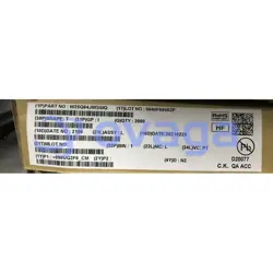
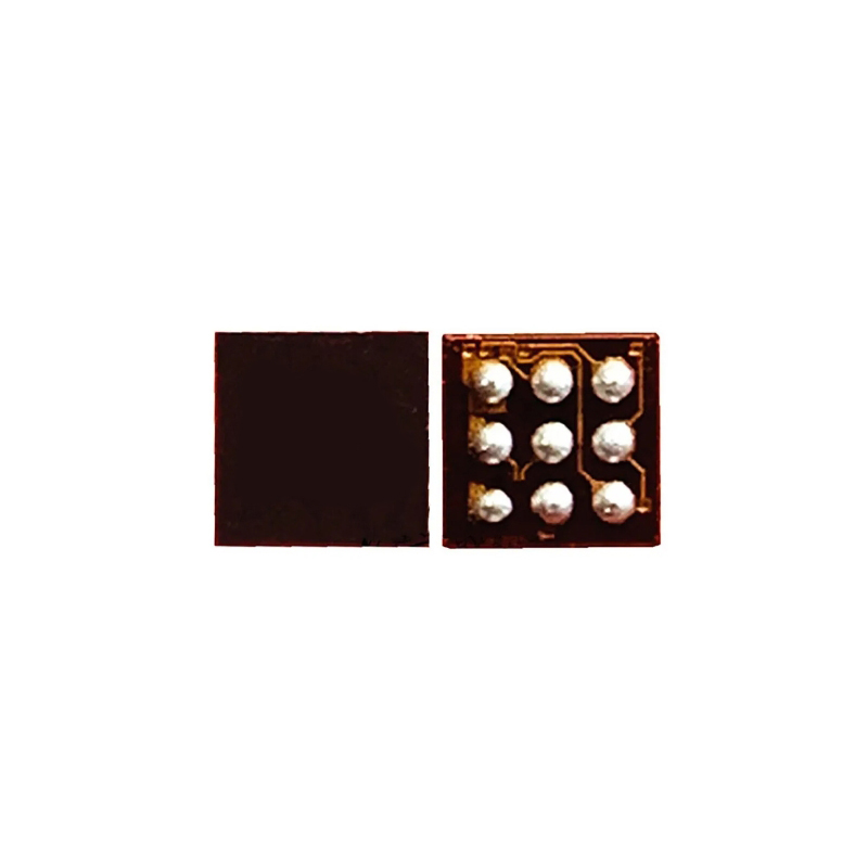
$5000WINBOND W631GG6KB15K
DRAM Chip DDR3 SDRAM 1Gbit 64Mx16 1.5V96-Pin WBGA


ブランド: WINBOND
製造元部品 #: W631GG6KB15K
データシート: W631GG6KB15K データシート (PDF)
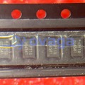
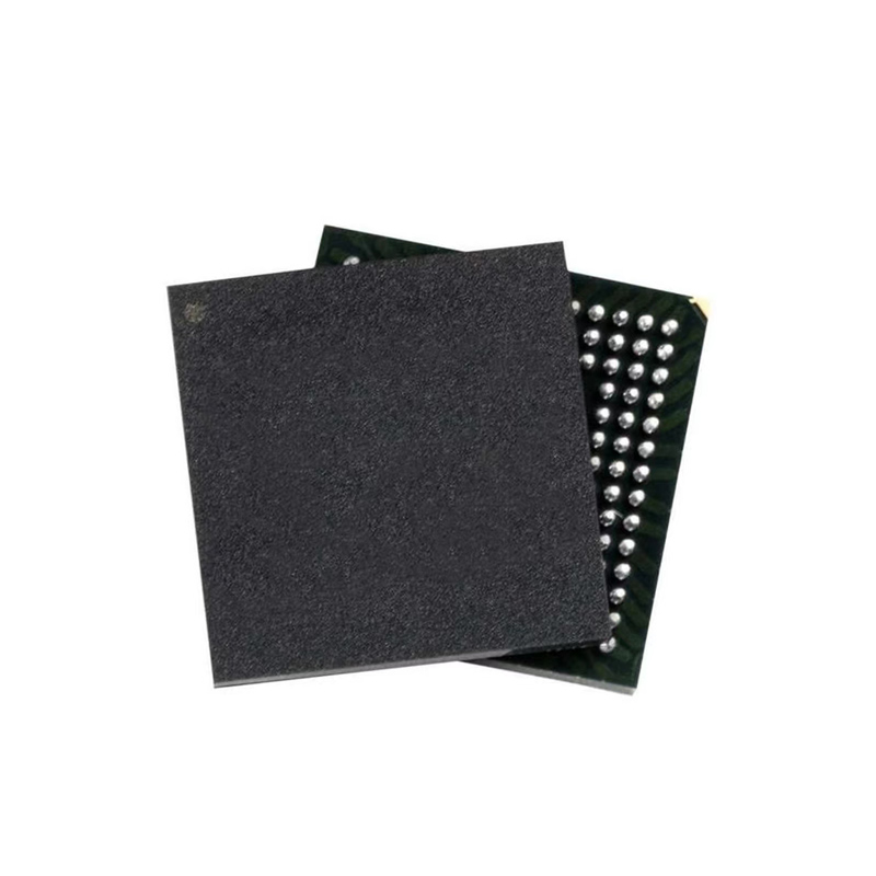
パッケージ/ケース: BGA
製品の種類: DRAM Chip
W631GG6KB15K 概要
GENERAL DESCRIPTIONThe W631GG6KB is a 1G bits DDR3 SDRAM, organized as 8,388,608 words x 8 banks x 16 bits. This device achieves high speed transfer rates up to 1866 Mb/sec/pin (DDR3-1866) for various applications. W631GG6KB is sorted into the following speed grades: -11, -12, 12I, 12A, 12K -15, 15I, 15A and 15K. The -11 speed grade is compliant to the DDR3-1866 (13-13-13) specification. The -12, 12I, 12A and 12K speed grades are compliant to the DDR3-1600 (11-11-11) specification (the 12I industrial grade which is guaranteed to support -40°C ≤ TCASE ≤ 95°C). The -15, 15I, 15A and 15K speed grades are compliant to the DDR3-1333 (9-9-9) specification (the 15I industrial grade which is guaranteed to support -40°C ≤ TCASE ≤ 95°C).FEATURES Power Supply: VDD, VDDQ = 1.5V ± 0.075V Double Data Rate architecture: two data transfers per clock cycle Eight internal banks for concurrent operation 8 bit prefetch architecture CAS Latency: 6, 7, 8, 9, 10, 11 and 13 Burst length 8 (BL8) and burst chop 4 (BC4) modes: fixed via mode register (MRS) or selectable On The-Fly (OTF) Programmable read burst ordering: interleaved or nibble sequential Bi-directional, differential data strobes (DQS and DQS#) are transmitted / received with data Edge-aligned with read data and center-aligned with write data DLL aligns DQ and DQS transitions with clock Differential clock inputs (CK and CK#) Commands entered on each positive CK edge, data and data mask are referenced to both edges of a differential data strobe pair (double data rate) Posted CAS with programmable additive latency (AL = 0, CL - 1 and CL - 2) for improved command, address and data bus efficiency Read Latency = Additive Latency plus CAS Latency (RL = AL + CL) Auto-precharge operation for read and write bursts Refresh, Self-Refresh, Auto Self-refresh (ASR) and Partial array self refresh (PASR) Precharged Power Down and Active Power Down
特徴
- Power Supply: VDD, VDDQ = 1.5V ± 0.075V
- Double Data Rate architecture: two data transfers per clock cycle
- Eight internal banks for concurrent operation
- 8 bit prefetch architecture
- CAS Latency: 6, 7, 8, 9, 10, 11 and 13
- Burst length 8 (BL8) and burst chop 4 (BC4) modes: fixed via mode register (MRS) or selectable On The-Fly (OTF)
- Programmable read burst ordering: interleaved or nibble sequential
- Bi-directional, differential data strobes (DQS and DQS#) are transmitted / received with data
- Edge-aligned with read data and center-aligned with write data
- DLL aligns DQ and DQS transitions with clock
- Differential clock inputs (CK and CK#)
- Commands entered on each positive CK edge, data and data mask are referenced to both edges of a differential data strobe pair (double data rate)
- Posted CAS with programmable additive latency (AL = 0, CL - 1 and CL - 2) for improved command, address and data bus efficiency
- Read Latency = Additive Latency plus CAS Latency (RL = AL + CL)
- Auto-precharge operation for read and write bursts
- Refresh, Self-Refresh, Auto Self-refresh (ASR) and Partial array self refresh (PASR)
- Precharged Power Down and Active Power Down
仕様
| パラメータ | 価値 | パラメータ | 価値 |
|---|---|---|---|
| EU RoHS | Yes | RoHS Version | 2011/65/EU, 2015/863 |
| ECCN | EAR99 | Automotive | Yes |
| Supplier Cage Code | SDM39 | HTSUSA | 8542320032 |
| Schedule B | 8542320015 |
配送
| 配送タイプ | 配送料 | リードタイム | |
|---|---|---|---|
 |
DHL | $20.00-$40.00 (0.50 KG) | 2-5 日々 |
 |
フェデックス | $20.00-$40.00 (0.50 KG) | 2-5 日々 |
 |
UPS | $20.00-$40.00 (0.50 KG) | 2-5 日々 |
 |
TNT | $20.00-$40.00 (0.50 KG) | 2-5 日々 |
 |
EMS | $20.00-$40.00 (0.50 KG) | 2-5 日々 |
 |
登録された航空便 | $20.00-$40.00 (0.50 KG) | 2-5 日々 |
処理時間:送料は地域や国によって異なります。
支払い
| 支払条件 | ハンドフィー | |
|---|---|---|
 |
電信送金 | 銀行手数料 US$30.00 を請求します。 |
 |
ペイパル | 4.0%のサービス料がかかります。 |
 |
クレジットカード | 3.5%のサービス料がかかります。 |
 |
ウエスタンユニオン | charge US.00 banking fee. |
 |
送金サービス | 銀行手数料は 0.00 米ドルかかります。 |
保証
1.購入した電子部品には365日保証が含まれており、製品の品質を保証します。
2.受け取った商品の一部が完璧な品質ではない場合、当社は責任を持って返金または交換を手配します。 ただし、商品は元の状態のままでなければなりません。
パッキング
-

ステップ1 :製品
-

ステップ2 :真空包装
-

ステップ3 :静電気防止袋
-

ステップ4 :個包装
-

ステップ5 :梱包箱
-

ステップ6 :バーコード配送タグ


すべての製品は静電気防止袋に梱包されます。 ESD 帯電防止保護を備えた状態で出荷されます。
社外の ESD 梱包ラベルには、部品番号、ブランド、数量などの当社の情報が使用されます。
私たちは出荷前にすべての商品を検査し、すべての製品が良好な状態であることを確認し、部品が新しいオリジナルでデータシートと一致していることを確認します。
すべての商品に問題がないことを確認した後、梱包後、安全に梱包し、グローバルエクスプレスで発送します。 優れた耐穿刺性と耐引裂性を示し、シールの完全性も良好です。


私たちは高品質の製品、思いやりのあるサービス、販売後の保証を提供します
-

豊富な商品を取り揃えておりますので、お客様の様々なニーズにお応え致します。
-

最小注文数量は1個からとなります。
-

最低国際配送料は0.00ドルから
-

全商品365日品質保証