


画像は参考用です。製品仕様を参照してください。
注文金額が
$5000
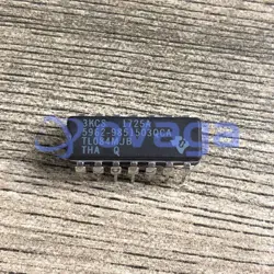
TI TLV9062QDRQ1

High-performance Dual Op Amp with Low Voltage Operation and Automotive-grade Reliability


ブランド: Texas Instruments
製造元部品 #: TLV9062QDRQ1
データシート: TLV9062QDRQ1 データシート (PDF)
パッケージ/ケース: SOIC (D)-8
RoHS ステータス:
在庫状況: 8,813 個、新しいオリジナル
製品の種類: Instrumentation, OP Amps, Buffer Amps
Warranty: 1 Year Ovaga Warranty - Find Out More
0
1
*すべての価格は米ドルです
| 数量 | 単価 | 外部価格 |
|---|---|---|
| 1 | $0.615 | $0.615 |
| 10 | $0.521 | $5.210 |
| 30 | $0.453 | $13.590 |
| 100 | $0.398 | $39.800 |
| 500 | $0.380 | $190.000 |
| 1000 | $0.369 | $369.000 |
在庫あり: 8,813 PCS
TLV9062QDRQ1 概要
Featuring a voltage range of 1.8 V to 5.5 V, the TLV9062QDRQ1 is specifically designed for low-voltage operation while delivering performance similar to the OPAx316 and TLVx316 devices. This makes it a reliable choice for automotive applications where space and power constraints are critical. The dual package design of the TLV9062-Q1 ensures that it can meet the needs of various circuit configurations, offering flexibility and efficiency
特徴
- Silicon fabrication process compliant
- Low power consumption optimized
- High-speed data transfer enabled
- Risk assessment and mitigation available
- System reliability ensured
- Temperature monitoring supported
応用
- Multi-industry usage
- Sensor signal conditioning
- Power efficiency
仕様
| パラメータ | 価値 | パラメータ | 価値 |
|---|---|---|---|
| Number of channels | 2 | Total supply voltage (+5 V = 5, ±5 V = 10) (max) (V) | 5.5 |
| Total supply voltage (+5 V = 5, ±5 V = 10) (min) (V) | 1.8 | Rail-to-rail | In, Out |
| GBW (typ) (MHz) | 10 | Slew rate (typ) (V/µs) | 6.5 |
| Vos (offset voltage at 25°C) (max) (mV) | 1.6 | Iq per channel (typ) (mA) | 0.538 |
| Vn at 1 kHz (typ) (nV√Hz) | 16 | Rating | Automotive |
| Operating temperature range (°C) | -40 to 125 | TI functional safety category | Functional Safety-Capable |
| Offset drift (typ) (µV/°C) | 0.53 | Features | Cost Optimized, EMI Hardened |
| CMRR (typ) (dB) | 103 | Iout (typ) (A) | 0.05 |
| Architecture | CMOS | Input common mode headroom (to negative supply) (typ) (V) | -0.1 |
| Input common mode headroom (to positive supply) (typ) (V) | 0.1 | Output swing headroom (to negative supply) (typ) (V) | 0.02 |
| Output swing headroom (to positive supply) (typ) (V) | -0.02 |
配送
| 配送タイプ | 配送料 | リードタイム | |
|---|---|---|---|
 |
DHL | $20.00-$40.00 (0.50 KG) | 2-5 日々 |
 |
フェデックス | $20.00-$40.00 (0.50 KG) | 2-5 日々 |
 |
UPS | $20.00-$40.00 (0.50 KG) | 2-5 日々 |
 |
TNT | $20.00-$40.00 (0.50 KG) | 2-5 日々 |
 |
EMS | $20.00-$40.00 (0.50 KG) | 2-5 日々 |
 |
登録された航空便 | $20.00-$40.00 (0.50 KG) | 2-5 日々 |
処理時間:送料は地域や国によって異なります。
支払い
| 支払条件 | ハンドフィー | |
|---|---|---|
 |
電信送金 | 銀行手数料 US$30.00 を請求します。 |
 |
ペイパル | 4.0%のサービス料がかかります。 |
 |
クレジットカード | 3.5%のサービス料がかかります。 |
 |
ウエスタンユニオン | charge US.00 banking fee. |
 |
送金サービス | 銀行手数料は 0.00 米ドルかかります。 |
保証
1.購入した電子部品には365日保証が含まれており、製品の品質を保証します。
2.受け取った商品の一部が完璧な品質ではない場合、当社は責任を持って返金または交換を手配します。 ただし、商品は元の状態のままでなければなりません。
パッキング
-

ステップ1 :製品
-

ステップ2 :真空包装
-

ステップ3 :静電気防止袋
-

ステップ4 :個包装
-

ステップ5 :梱包箱
-

ステップ6 :バーコード配送タグ


すべての製品は静電気防止袋に梱包されます。 ESD 帯電防止保護を備えた状態で出荷されます。
社外の ESD 梱包ラベルには、部品番号、ブランド、数量などの当社の情報が使用されます。
私たちは出荷前にすべての商品を検査し、すべての製品が良好な状態であることを確認し、部品が新しいオリジナルでデータシートと一致していることを確認します。
すべての商品に問題がないことを確認した後、梱包後、安全に梱包し、グローバルエクスプレスで発送します。 優れた耐穿刺性と耐引裂性を示し、シールの完全性も良好です。


パーツポイント
-
The TLV9062QDRQ1 is a high-precision, low-power operational amplifier designed for automotive applications. It features low offset voltage, low noise, and a wide supply voltage range, making it suitable for sensor interfaces, signal conditioning, and precision measurements in automotive systems. This chip also offers short circuit and thermal protection to ensure reliable operation in harsh environments.
-
Equivalent
Some equivalent products to the TLV9062QDRQ1 chip are the AD8532ARZ, MAX44267ASA, and MCP602-I/P. These chips offer similar functionality and characteristics, making them suitable replacements for the TLV9062QDRQ1 in various applications. -
Features
TLV9062QDRQ1 is a dual, high-speed, low-power operational amplifier with rail-to-rail input and output. It has a wide supply voltage range of 1.8V to 5.5V, low quiescent current of 650uA, and low noise of 12nV/√Hz. It is suitable for automotive applications and operates over a wide temperature range of -40°C to 125°C. -
Pinout
The TLV9062QDRQ1 is a dual operational amplifier with rail-to-rail output and low offset voltage. It has a pin count of 8. Pin functions include VCC-, OUT1, IN-, IN+, VCC+, OUT2, GND, and NC. -
Manufacturer
TLV9062QDRQ1 is manufactured by Texas Instruments Incorporated, a multinational semiconductor company based in Dallas, Texas. Texas Instruments specializes in designing and manufacturing semiconductors and integrated circuits for a variety of applications, including analog and embedded processing products. -
Application Field
TLV9062QDRQ1 is typically used in automotive applications such as body control modules, HVAC systems, and powertrain control modules. It is also suitable for industrial automation, consumer electronics, and communication systems due to its low power consumption, rail-to-rail input/output, and wide input voltage range capabilities. -
Package
The TLV9062QDRQ1 chip comes in a SOIC-8 package, with dimensions of 3.9mm x 4.9mm x 1.75mm. It is a dual operational amplifier with 1.8V to 5.5V operating voltage range and rail-to-rail input/output.


私たちは高品質の製品、思いやりのあるサービス、販売後の保証を提供します
-

豊富な商品を取り揃えておりますので、お客様の様々なニーズにお応え致します。
-

最小注文数量は1個からとなります。
-

最低国際配送料は0.00ドルから
-

全商品365日品質保証


