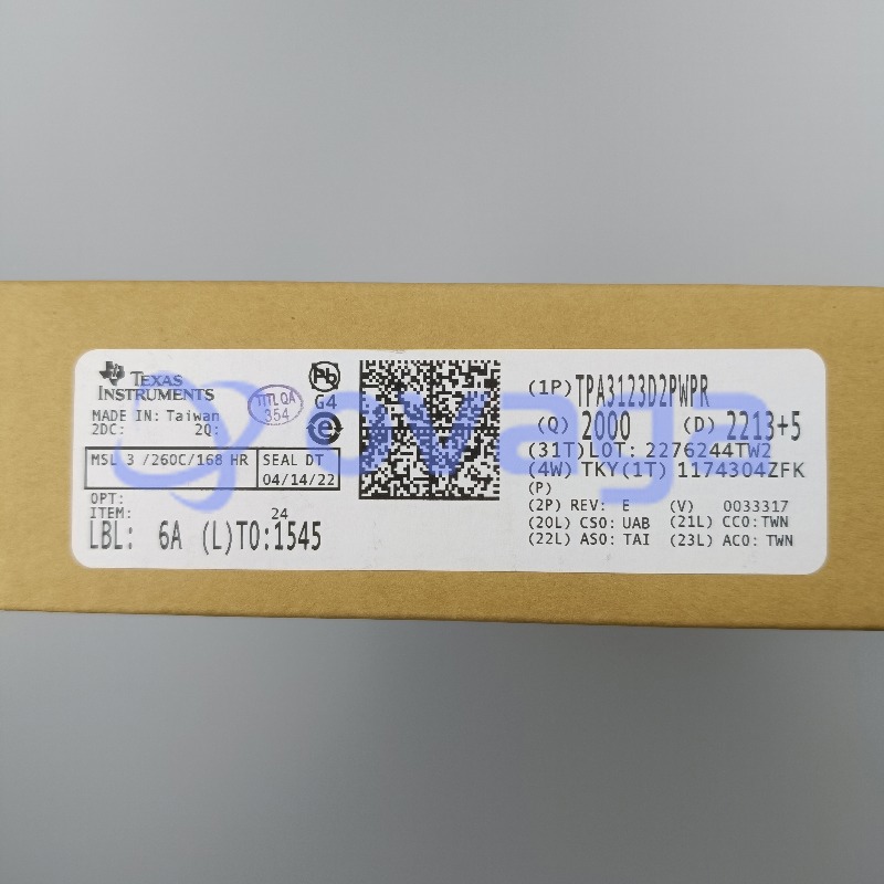
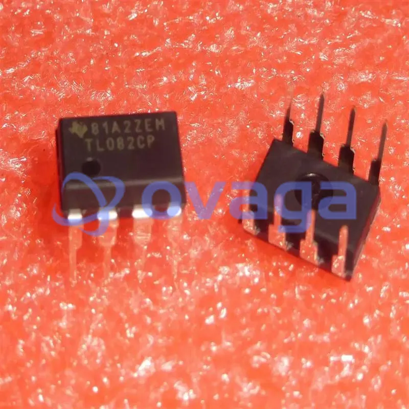
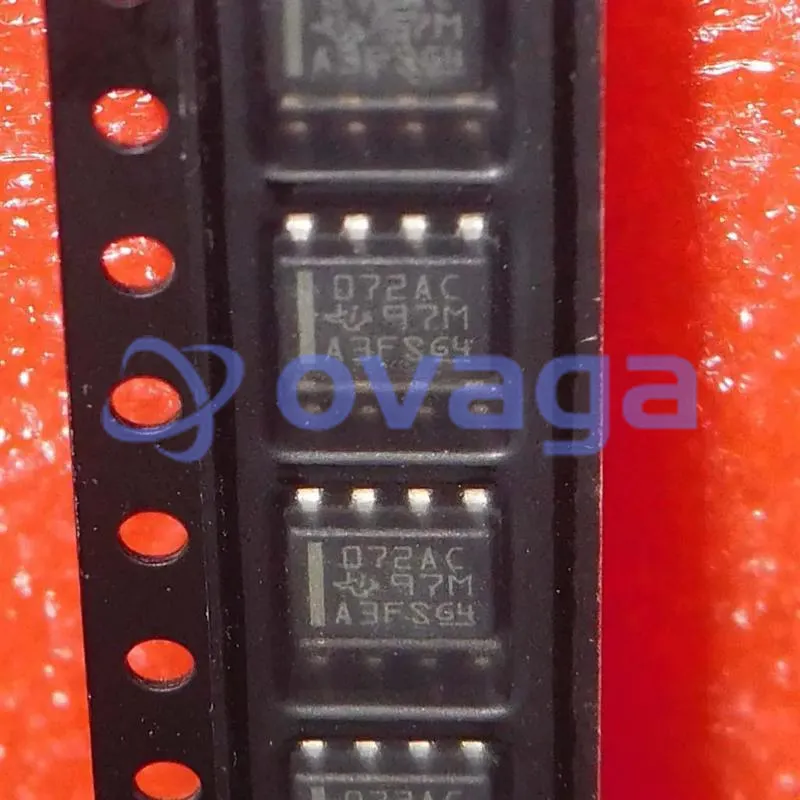
画像は参考用です。製品仕様を参照してください。
TI TLC27M4BIN
Precision Amplifiers LiNCMOS Med Bias


ブランド: Texas Instruments
製造元部品 #: TLC27M4BIN
データシート: TLC27M4BIN データシート (PDF)
パッケージ/ケース: 14-PDIP
RoHS ステータス:
在庫状況: 9718 個、新しいオリジナル
製品の種類: Precision Amplifiers
0
1
*すべての価格は米ドルです
| 数量 | 単価 | 外部価格 |
|---|---|---|
| 1 | $4.780 | $4.780 |
| 200 | $1.851 | $370.200 |
| 500 | $1.787 | $893.500 |
| 1000 | $1.753 | $1753.000 |
In Stock:9718 PCS
TLC27M4BIN 概要
The TLC27M4 and TLC27M9 quad operational amplifiers combine a wide range of input offset voltage grades with low offset voltage drift, high input impedance, low noise, and speeds comparable to that of general-purpose bipolar devices.These devices use Texas Instruments silicon-gate LinCMOSTM
LinCMOS is a trademark of Texas Instruments Incorporated. technology, which provides offset voltage stability far exceeding the stability available with conventional metal-gate processes.
The extremely high input impedance, low bias currents, make these cost-effective devices ideal for applications that have previously been reserved for general-purpose bipolar products, but with only a fraction of the power consumption.
Four offset voltage grades are available (C-suffix and I-suffix types), ranging from the low-cost TLC27M4 (10 mV) to the high-precision TLC27M9 (900 uV). These advantages, in combination with good common-mode rejection and supply voltage rejection, make these devices a good choice for new state-of-the-art designs as well as for upgrading existing designs.
In general, many features associated with bipolar technology are available on LinCMOSTM operational amplifiers, without the power penalties of bipolar technology. General applications such as transducer interfacing, analog calculations, amplifier blocks, active filters, and signal buffering are easily designed with the TLC27M4 and TLC27M9. The devices also exhibit low voltage single-supply operation, and low power consumption, making them ideally suited for remote and inaccessible battery-powered applications. The common-mode input voltage range includes the negative rail.
A wide range of packaging options is available, including small-outline and chip-carrier versions for high-density system applications.
The device inputs and outputs are designed to withstand -100-mA surge currents without sustaining latch-up.
The TLC27M4 and TLC27M9 incorporate internal ESD-protection circuits that prevent functional failures at voltages up to 2000 V as tested under MIL-STD-883C, Method 3015; however, care should be exercised in handling these devices, as exposure to ESD may result in the degradation of the device parametric performance.
The C-suffix devices are characterized for operation from 0°C to 70°C. The I-suffix devices are characterized for operation from -40°C to 85°C. The M-suffix devices are characterized for operation over the full military temperature range of -55°C to 125°C.
AVAILABLE OPTIONS TAVIOmax
AT 25°C
PACKAGE
CHIP
FORM
(Y) SMALL OUTLINE
(D)
CHIP CARRIER
(FK)
CERAMIC DIP
(J)
PLASTIC DIP
(N)
TSSOP
(PW)
0°C to 70°C
900 uV
TLC27M9CD
--
--
TLC27M9CN
--
--
2 mV
TLC27M4BCD
--
--
TLC27M4BCN
--
--
5 mV
TLC27M4ACD
--
--
TLC27M4ACN
--
--
10 mV
TLC27M4CD
--
--
TLC27M4CN
TLC27M4CPW
TLC27M4Y
-40°C to 85°C
900 uV
TLC27M9ID
--
--
TLC27M9IN
--
--
2 mV
TLC27M4BID
--
--
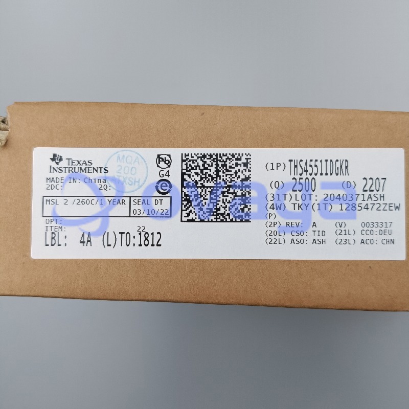
TLC27M4BIN
--
--
5 mV
TLC27M4AID
--
--
TLC27M4AIN
--
--
10 mV
TLC27M4ID
--
--
TLC27M4IN
TLC27M41PW
--
-55°C to 125°C
900 uV
TLC27M9MD
TLC27M9MFK
TLC27M9MJ
TLC27M9MN
--
--
10 mV
TLC27M4MD
TLC27M4MFK
TLC27M4MJ
TLC27M4MN
--
--
The D and PW package is available taped and reeled. Add R suffix to the device type (e.g., TLC279CDR).
特徴
- Trimmed Offset Voltage:
TLC27M9.900 uV Max at TA = 25°C,
VDD = 5 V - Input Offset Voltage Drift.Typically
0.1 uV/Month, Including the First 30 Days - Wide Range of Supply Voltages Over Specified Temperature Range:
0°C to 70°C.3 V to 16 V
-40°C to 85°C.4 V to 16 V
-55°C to 125°C.4 V to 16 V - Single-Supply Operation
- Common-Mode Input Voltage Range Extends Below the Negative Rail (C-Suffix, I-Suffix Types)
- Low Noise.Typically 32 nV/ Hz\
at f = 1 kHz - Low Power.Typically 2.1 mW at TA=25°C, VDD = 5 V
- Output Voltage Range Includes Negative Rail
- High Input Impedance.1012 Typ
- ESD-Protection Circuitry
- Small-Outline Package Option Also Available in Tape and Reel
- Designed-In Latch-Up Immunity
仕様
| パラメータ | 価値 | パラメータ | 価値 |
|---|---|---|---|
| Manufacturer | Texas Instruments | Product Category | Precision Amplifiers |
| RoHS | Details | Series | TLC27M4B |
| Number of Channels | 4 Channel | GBP - Gain Bandwidth Product | 525 kHz |
| SR - Slew Rate | 620 mV/us | CMRR - Common Mode Rejection Ratio | 91 dB |
| Output Current per Channel | 30 mA | Ib - Input Bias Current | 0.7 pA |
| Vos - Input Offset Voltage | 260 uV | en - Input Voltage Noise Density | 32 nV/sqrt Hz |
| Supply Voltage - Max | 16 V | Supply Voltage - Min | 4 V |
| Operating Supply Current | 570 uA | Minimum Operating Temperature | - 40 C |
| Maximum Operating Temperature | + 85 C | Shutdown | No Shutdown |
| Mounting Style | SMD/SMT | Package / Case | PDIP-14 |
| Amplifier Type | Precision Amplifier | Brand | Texas Instruments |
| Height | 4.57 mm | Input Type | Rail-to-Rail |
| Ios - Input Offset Current | 1 nA | Length | 19.3 mm |
| Operating Supply Voltage | 4 V to 16 V | Pd - Power Dissipation | 1.575 W |
| Product | Precision Amplifiers | Product Type | Precision Amplifiers |
| Factory Pack Quantity | 25 | Subcategory | Amplifier ICs |
| Supply Type | Single | Technology | LinCMOS |
| Tradename | LinCMOS | Vcm - Common Mode Voltage | Negative Rail - 0.2 V to Positive Rail - 1 V |
| Width | 6.35 mm |
配送
| 配送タイプ | 配送料 | リードタイム | |
|---|---|---|---|
 |
DHL | $20.00-$40.00 (0.50 KG) | 2-5 日々 |
 |
フェデックス | $20.00-$40.00 (0.50 KG) | 2-5 日々 |
 |
UPS | $20.00-$40.00 (0.50 KG) | 2-5 日々 |
 |
TNT | $20.00-$40.00 (0.50 KG) | 2-5 日々 |
 |
EMS | $20.00-$40.00 (0.50 KG) | 2-5 日々 |
 |
登録された航空便 | $20.00-$40.00 (0.50 KG) | 2-5 日々 |
処理時間:送料は地域や国によって異なります。
支払い
| 支払条件 | ハンドフィー | |
|---|---|---|
 |
電信送金 | 銀行手数料 US$30.00 を請求します。 |
 |
ペイパル | 4.0%のサービス料がかかります。 |
 |
クレジットカード | 3.5%のサービス料がかかります。 |
 |
ウエスタンユニオン | charge US.00 banking fee. |
 |
送金サービス | 銀行手数料は 0.00 米ドルかかります。 |
保証
1.購入した電子部品には365日保証が含まれており、製品の品質を保証します。
2.受け取った商品の一部が完璧な品質ではない場合、当社は責任を持って返金または交換を手配します。 ただし、商品は元の状態のままでなければなりません。
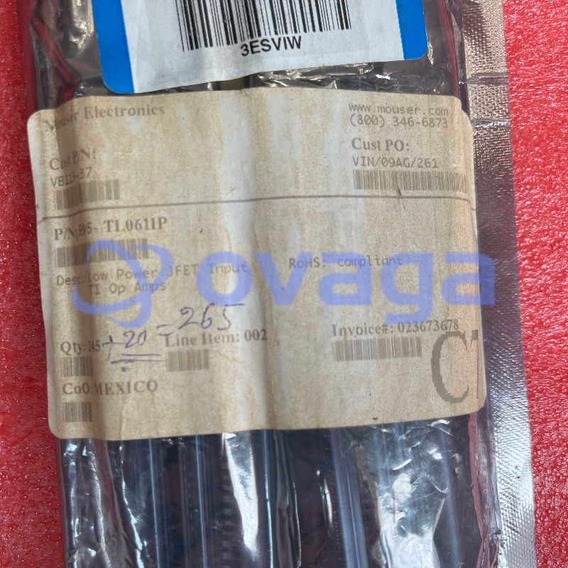
パッキング
-

ステップ1 :製品
-

ステップ2 :真空包装
-

ステップ3 :静電気防止袋
-

ステップ4 :個包装
-

ステップ5 :梱包箱
-

ステップ6 :バーコード配送タグ
すべての製品は静電気防止袋に梱包されます。 ESD 帯電防止保護を備えた状態で出荷されます。
社外の ESD 梱包ラベルには、部品番号、ブランド、数量などの当社の情報が使用されます。
私たちは出荷前にすべての商品を検査し、すべての製品が良好な状態であることを確認し、部品が新しいオリジナルでデータシートと一致していることを確認します。
すべての商品に問題がないことを確認した後、梱包後、安全に梱包し、グローバルエクスプレスで発送します。 優れた耐穿刺性と耐引裂性を示し、シールの完全性も良好です。


私たちは高品質の製品、思いやりのあるサービス、販売後の保証を提供します
-

豊富な商品を取り揃えておりますので、お客様の様々なニーズにお応え致します。
-

最小注文数量は1個からとなります。
-

最低国際配送料は0.00ドルから
-

全商品365日品質保証