画像は参考用です。製品仕様を参照してください。
注文金額が
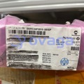
$5000PIC24FJ64GA406-I/MR
Low Power MCU with Security & Segmented LCD.


ブランド: Microchip
製造元部品 #: PIC24FJ64GA406-I/MR
データシート: PIC24FJ64GA406-I/MR データシート (PDF)
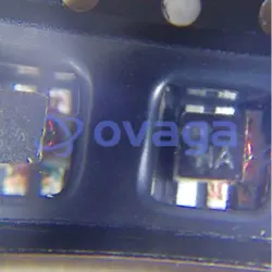
パッケージ/ケース: QFN-64
製品の種類: Microcontrollers
PIC24FJ64GA406-I/MR 概要
For developers looking to incorporate advanced security features into their embedded systems, the PIC24FJ64GA406-I/MR offers a compelling solution. With its integrated crypto module and eXtreme Low Power capabilities, this 16-bit microcontroller is well-equipped to handle the demands of modern security applications. Its 64KB Flash memory, 8KB RAM, and segmented LCD provide ample resources for storing data and interacting with users. Whether you're designing a secure access control system, a payment terminal, or a data logging device, this microcontroller delivers the performance and features needed to meet your project requirements
特徴
- Cryptographic Engine
- Performs NIST Standard Encryption/Decryption Operations without CPU Intervention
- AES Cipher Support for 128, 192 and 256-Bit Keys
- DES/3DES Cipher Support, with up to Three Unique Keys for 3DES
- Supports ECB, CBC, OFB, CTR and CFB128 modes
- Programmatically Secure OTP Array for Key Storage
- True Random Number Generation
- Battery-Backed RAM Key Storage
- Extreme Low Power
- Multiple Power Management Options for Extreme Power Reduction:
- VBAT allows for lowest power consumption on backup battery (with or without RTCC)
- Deep Sleep allows near total power-down with the ability to wake-up on external triggers
- Sleep and Idle modes selectively shut down peripherals and/or core for substantial power reduction and fast wake-up
- Doze mode allows CPU to run at a lower clock speed than peripherals
- Alternate Clock modes allow On-the-Fly Switching to a Lower Clock Speed for Selective Power Reduction
- Extreme Low-Power Current Consumption for Deep Sleep WDT: 650 nA @ 2V typical RTCC: 650 nA @ 32 kHz, 2V typical Deep Sleep current, 60 nA typical
- 160 uA/MHz in Run mode
- CPU
- Modified Harvard Architecture
- Up to 16 MIPS Operation @ 32 MHz
- 8 MHz Internal Oscillator: 96 MHz PLL / Multiple clock divide options / Fast start-up
- 17-Bit x 17-Bit Single-Cycle Hardware Fractional/Integer Multiplier
- 32-Bit by 16-Bit Hardware Divider
- 16 x 16-Bit Working Register Array
- C Compiler Optimized Instruction Set Architecture
- Two Address Generation Units for Separate Read and Write Addressing of Data Memory
- Analog Features
- 10/12-Bit, up to 24-Channel Analog-to-Digital (A/D) Converter:
- Conversion rate of 500 ksps (10-bit), 200 kbps (12-bit)
- Auto-scan and threshold compare features
- Conversion available during Sleep
- One 10-Bit Digital-to-Analog Converter (DAC): 1Msps update rate
- Three Rail-to-Rail, Enhanced Analog Comparators with Programmable Input/Output Configuration
- Charge Time Measurement Unit (CTMU) for cap touch or precise time measurement
- Dual Partition Flash with Live Update Capability
- Capable of Holding Two Independent Software Applications, including Bootloader
- Permits Simultaneous Programming of One Partition while Executing Application Code from the Other
- Allows Run-Time Switching Between Active Partitions
仕様
| パラメータ | 価値 | パラメータ | 価値 |
|---|---|---|---|
| CPU Type | 16-bit PIC MCU | CPU Speed (MHz) | 16 |
| Program Memory Size (KB) | 64 | Multiple Flash Panels | Yes |
| Direct Memory Access (DMA) Channels | 6 | Temp. Range Min.(C°) | -40 |
| Temp. Range Max.(C°) | 85 | Operation Voltage Min.(V) | 2 |
| Operation Voltage Max.(V) | 3.6 | Pin Count | 64 |
| Low Power | Yes | Number of Comparators | 3 |
| Number of ADCs | 1 | ADC Channels | 16 |
| Max ADC Resolution (bits) | 12 | Max ADC Sampling Rate (ksps) | 500 |
| Number of DACs | 1 | DAC outputs | 1 |
| Max DAC Resolution (bits) | 10 | Hardware RTCC | Yes |
| Motor Control PWM Channels | 0 | SMPS PWM Channels | 0 |
| Number of PWM Time Bases | 1 | Output Compare Channels | 6 |
| USB Interface | None | Number of CAN Modules | 0 |
| Type of CAN module | None | Crypto Engine | Yes |
| Quadrature Encoder Interface (QEI) | 0 | Segment LCD | 248 |
| LCD/Graphics Interface | No | Configurable Logic Cell Modules (CLC /CCL) | 4 |
| Peripheral Pin Select (PPS)/Pin Muxing | Yes |
配送
| 配送タイプ | 配送料 | リードタイム | |
|---|---|---|---|
 |
DHL | $20.00-$40.00 (0.50 KG) | 2-5 日々 |
 |
フェデックス | $20.00-$40.00 (0.50 KG) | 2-5 日々 |
 |
UPS | $20.00-$40.00 (0.50 KG) | 2-5 日々 |
 |
TNT | $20.00-$40.00 (0.50 KG) | 2-5 日々 |
 |
EMS | $20.00-$40.00 (0.50 KG) | 2-5 日々 |
 |
登録された航空便 | $20.00-$40.00 (0.50 KG) | 2-5 日々 |
処理時間:送料は地域や国によって異なります。
支払い
| 支払条件 | ハンドフィー | |
|---|---|---|
 |
電信送金 | 銀行手数料 US$30.00 を請求します。 |
 |
ペイパル | 4.0%のサービス料がかかります。 |
 |
クレジットカード | 3.5%のサービス料がかかります。 |
 |
ウエスタンユニオン | charge US.00 banking fee. |
 |
送金サービス | 銀行手数料は 0.00 米ドルかかります。 |
保証
1.購入した電子部品には365日保証が含まれており、製品の品質を保証します。
2.受け取った商品の一部が完璧な品質ではない場合、当社は責任を持って返金または交換を手配します。 ただし、商品は元の状態のままでなければなりません。
パッキング
-

ステップ1 :製品
-

ステップ2 :真空包装
-

ステップ3 :静電気防止袋
-

ステップ4 :個包装
-

ステップ5 :梱包箱
-

ステップ6 :バーコード配送タグ


すべての製品は静電気防止袋に梱包されます。 ESD 帯電防止保護を備えた状態で出荷されます。
社外の ESD 梱包ラベルには、部品番号、ブランド、数量などの当社の情報が使用されます。
私たちは出荷前にすべての商品を検査し、すべての製品が良好な状態であることを確認し、部品が新しいオリジナルでデータシートと一致していることを確認します。
すべての商品に問題がないことを確認した後、梱包後、安全に梱包し、グローバルエクスプレスで発送します。 優れた耐穿刺性と耐引裂性を示し、シールの完全性も良好です。


私たちは高品質の製品、思いやりのあるサービス、販売後の保証を提供します
-

豊富な商品を取り揃えておりますので、お客様の様々なニーズにお応え致します。
-

最小注文数量は1個からとなります。
-

最低国際配送料は0.00ドルから
-

全商品365日品質保証