

画像は参考用です。製品仕様を参照してください。
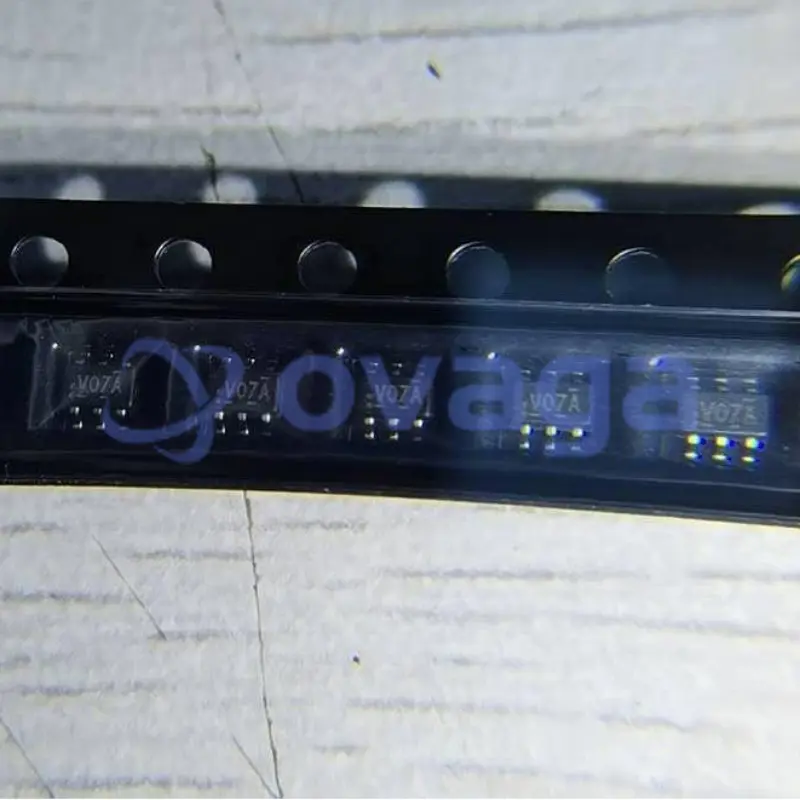
ON NC7WV07P6X
Buffer, Non-Inverting 2 Element 1 Bit per Element Open Drain Output SC-88 (SC-70-6)


ブランド: ON Semiconductor, LLC
製造元部品 #: NC7WV07P6X
データシート: NC7WV07P6X Datasheet (PDF)
パッケージ/ケース: SC-70-6
製品の種類: ロジックIC
NC7WV07P6X 概要
The NC7WV07 is a dual buffer with open drain output from ON Semiconductor's Ultra Low Power-A series of TinyLogic®. ULP-A is ideal for applications that require extreme high speed, high drive and low power. This product is designed for a wide low voltage operating range (0.9V to 3.6V VCC) and applications that require more drive and speed than the TinyLogic ULP series, but still offer best in class low power operation.
The NC7WV07 is uniquely designed for optimized power and speed, and is fabricated with an advanced CMOS technology to achieve high-speed operation while maintaining low CMOS power dissipation.
特徴
- 0.9V to 3.6V VCC supply operation
- 3.6V overvoltage tolerant I/O's at VCC from 0.9V to 3.6V
- Extremely High Speed tPD1.0 ns typ for 2.7V to 3.6V VCC1.2 ns typ for 2.3V to 2.7V VCC2.0 ns typ for 1.65V to 1.95V VCC3.2 ns typ for 1.4V to 1.6V VCC6.0 ns typ for 1.1V to 1.3V VCC13.0 ns typ for 0.9V VCC
- Power-Off high impedance inputs and outputs
- High Static Drive (IOH/IOL)±24 mA @ 3.00V VCC±18 mA @ 2.30V VCC±6 mA @ 1.65V VCC±4 mA @ 1.4V VCC±2 mA @ 1.1V VCC±0.1 mA @ 0.9V VCC
- Uses patented Quiet Series™ noise/EMI reduction circuitry
- Ultra small MicroPak™ leadfree package
- Ultra low dynamic power
応用
- This product is general usage and suitable for many different applications.
仕様
| パラメータ | 価値 | パラメータ | 価値 |
|---|---|---|---|
| Source Content uid | NC7WV07P6X | Pbfree Code | Yes |
| Part Life Cycle Code | Active | Ihs Manufacturer | ONSEMI |
| Package Description | SC-88, 6 PIN | Manufacturer Package Code | 419AD |
| Reach Compliance Code | compliant | HTS Code | 8542.39.00.01 |
| Factory Lead Time | 75 Weeks, 5 Days | Samacsys Manufacturer | onsemi |
| Family | AUP/ULP/V | JESD-30 Code | R-PDSO-G6 |
| Logic IC Type | BUFFER | Moisture Sensitivity Level | 1 |
| Number of Functions | 2 | Number of Inputs | 1 |
| Number of Terminals | 6 | Output Characteristics | OPEN-DRAIN |
| Package Body Material | PLASTIC/EPOXY | Package Code | TSSOP |
| Package Equivalence Code | TSSOP6,.08 | Package Shape | RECTANGULAR |
| Package Style | SMALL OUTLINE, THIN PROFILE, SHRINK PITCH | Packing Method | TR |
| Peak Reflow Temperature (Cel) | 260 | Schmitt Trigger | NO |
| Surface Mount | YES | Technology | CMOS |
| Terminal Finish | NICKEL PALLADIUM GOLD | Terminal Form | GULL WING |
| Terminal Position | DUAL | Time@Peak Reflow Temperature-Max (s) | 30 |
| feature-logic-family | WV | feature-logic-function | Buffer/Driver |
| feature-number-of-elements-per-chip | 2 | feature-process-technology | CMOS |
| feature-maximum-low-level-output-current-ma | 24 | feature-output-type | Open Drain |
| feature-minimum-operating-supply-voltage-v | 0.9 | feature-maximum-operating-supply-voltage-v | 3.6 |
| feature-maximum-high-level-output-current-ma | -24 | feature-packaging | Tape and Reel |
| feature-rad-hard | feature-pin-count | 6 | |
| feature-supplier-package | SC-70 | feature-standard-package-name1 | SOT |
| feature-cecc-qualified | No | feature-esd-protection | |
| feature-military | No | feature-aec-qualified | No |
| feature-aec-qualified-number | feature-auto-motive | No | |
| feature-p-pap | No | feature-eccn-code | EAR99 |
| feature-svhc | No |
配送
| 配送タイプ | 配送料 | リードタイム | |
|---|---|---|---|
 |
DHL | $20.00-$40.00 (0.50 KG) | 2-5 日々 |
 |
フェデックス | $20.00-$40.00 (0.50 KG) | 2-5 日々 |
 |
UPS | $20.00-$40.00 (0.50 KG) | 2-5 日々 |
 |
TNT | $20.00-$40.00 (0.50 KG) | 2-5 日々 |
 |
EMS | $20.00-$40.00 (0.50 KG) | 2-5 日々 |
 |
登録された航空便 | $20.00-$40.00 (0.50 KG) | 2-5 日々 |
処理時間:送料は地域や国によって異なります。
支払い
| 支払条件 | ハンドフィー | |
|---|---|---|
 |
電信送金 | 銀行手数料 US$30.00 を請求します。 |
 |
ペイパル | 4.0%のサービス料がかかります。 |
 |
クレジットカード | 3.5%のサービス料がかかります。 |
 |
ウエスタンユニオン | charge US.00 banking fee. |
 |
送金サービス | 銀行手数料は 0.00 米ドルかかります。 |
保証
1.購入した電子部品には365日保証が含まれており、製品の品質を保証します。
2.受け取った商品の一部が完璧な品質ではない場合、当社は責任を持って返金または交換を手配します。 ただし、商品は元の状態のままでなければなりません。
パッキング
-

ステップ1 :製品
-

ステップ2 :真空包装
-

ステップ3 :静電気防止袋
-

ステップ4 :個包装
-

ステップ5 :梱包箱
-

ステップ6 :バーコード配送タグ


すべての製品は静電気防止袋に梱包されます。 ESD 帯電防止保護を備えた状態で出荷されます。
社外の ESD 梱包ラベルには、部品番号、ブランド、数量などの当社の情報が使用されます。
私たちは出荷前にすべての商品を検査し、すべての製品が良好な状態であることを確認し、部品が新しいオリジナルでデータシートと一致していることを確認します。
すべての商品に問題がないことを確認した後、梱包後、安全に梱包し、グローバルエクスプレスで発送します。 優れた耐穿刺性と耐引裂性を示し、シールの完全性も良好です。


パーツポイント
-
The NC7WV07P6X chip is a triple buffer gate that can be used for level shifting signals in various electronic circuits. It has three inputs and three outputs and operates at a supply voltage of 1.65V to 5.5V. The chip is designed to provide high-speed signal buffering while consuming very low power, making it suitable for applications in portable devices and battery-powered systems.
-
Equivalent
There aren't any exact equivalent products to the NC7WV07P6X chip. However, some similar alternatives you may consider are the SN74LV07A, TC7WG07FK, and HCT07 chips, as they have similar functionalities and specifications. -
Features
The NC7WV07P6X is a dual buffer/line driver that operates from rail-to-rail voltage signals with a wide operating voltage range. It offers low power consumption, high-speed operation, and is designed with Schmitt-trigger inputs to provide noise immunity. It also has balanced input and output characteristics and supports overvoltage-tolerant input levels, making it suitable for various applications. -
Pinout
The NC7WV07P6X is a single logic gate with an open-drain output. It has a pin count of 6, which includes one input pin, one output pin, and four power supply/GND pins. The open-drain output allows for bi-directional signal transmission and is commonly used for level shifting applications. -
Manufacturer
The manufacturer of the NC7WV07P6X is ON Semiconductor. ON Semiconductor is a multinational company specializing in the design and production of semiconductors and integrated circuits for various industries, including automotive, communications, computing, and consumer electronics. -
Application Field
The NC7WV07P6X is a voltage-level translator used for translating voltage levels between different logic families. It can be applied in various applications such as battery-powered portable devices, mobile phones, digital cameras, and other electronics requiring voltage translation between different logic levels. -
Package
The NC7WV07P6X chip has a package type of SC-70, a form of SMD (Surface Mount Device), and a size of 2.00mm x 2.10mm x 1.20mm.


データシート PDF
私たちは高品質の製品、思いやりのあるサービス、販売後の保証を提供します
-

豊富な商品を取り揃えておりますので、お客様の様々なニーズにお応え致します。
-

最小注文数量は1個からとなります。
-

最低国際配送料は0.00ドルから
-

全商品365日品質保証


We will definitely be purchasing from Ovaga in the future.