


画像は参考用です。製品仕様を参照してください。
注文金額が
$5000ON NB3L553MNR4G
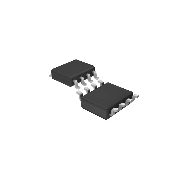
Clock Fanout Buffer (Distribution) IC 1:4 200 MHz 8-VFDFN Exposed Pad


ブランド: ON Semiconductor, LLC
製造元部品 #: NB3L553MNR4G
データシート: NB3L553MNR4G Datasheet (PDF)
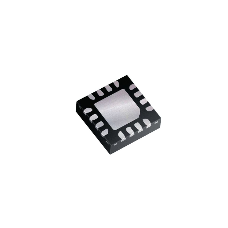
パッケージ/ケース: DFN-8 EP
製品の種類: Clock Buffers, Drivers
NB3L553MNR4G 概要
The NB3L553MNR4G clock fanout buffer is a versatile integrated circuit with a frequency of 200MHz, offering 4 outputs for efficient distribution of clock signals in electronic systems. With a supply voltage range of 2.375V to 5.25V, this fanout buffer can accommodate a wide range of system requirements. The DFN-8 case style and 8 pins allow for easy integration into circuit designs, while the operating temperature range of -40°C to 85°C makes it suitable for use in challenging environmental conditions. In addition, this clock fanout buffer is RoHS phthalates compliant and MSL 1 - unlimited, ensuring it meets industry standards for environmental and manufacturing safety
特徴
- Schmitt trigger input with hysteresis
- Output can drive heavy loads
- VCC pin can be tied to GND for shutdown
応用
- Reliable choice for data transmission
- Efficient solution for networking needs
- Enhance your digital communication
仕様
| パラメータ | 価値 | パラメータ | 価値 |
|---|---|---|---|
| Status | Active | CAD Models | |
| Compliance | PbAHP | Package Type | DFN-8 |
| Case Outline | 506AA | MSL Type | 1 |
| MSL Temp (°C) | 260 | Container Type | REEL |
| Container Qty. | 1000 | ON Target | Y |
| Type | Buffer | Channels | 1 |
| Input / Output Ratio | 1:4 | Input Level | CMOS |
| Output Level | CMOS | VCC Typ (V) | 5 |
| tJitterRMS Typ (ps) | 0.029 | tskew(o-o) Max (ps) | 50 |
| tpd Typ (ns) | 3 | tR & tF Max (ps) | 700 |
| fmaxClock Typ (MHz) | 200 | fmaxData Typ (Mbps) | - |
| Pricing ($/Unit) | Price N/A | feature-maximum-operating-supply-voltage-v | 5.25 |
| feature-minimum-operating-supply-voltage-v | 2.375 | feature-packaging | Tape and Reel |
| feature-rad-hard | feature-pin-count | 8 | |
| feature-supplier-package | DFN EP | feature-standard-package-name1 | DFN |
| feature-cecc-qualified | No | feature-esd-protection | Yes |
| feature-military | No | feature-aec-qualified | No |
| feature-aec-qualified-number | feature-auto-motive | No | |
| feature-p-pap | No | feature-eccn-code | EAR99 |
| feature-svhc | No |
配送
| 配送タイプ | 配送料 | リードタイム | |
|---|---|---|---|
 |
DHL | $20.00-$40.00 (0.50 KG) | 2-5 日々 |
 |
フェデックス | $20.00-$40.00 (0.50 KG) | 2-5 日々 |
 |
UPS | $20.00-$40.00 (0.50 KG) | 2-5 日々 |
 |
TNT | $20.00-$40.00 (0.50 KG) | 2-5 日々 |
 |
EMS | $20.00-$40.00 (0.50 KG) | 2-5 日々 |
 |
登録された航空便 | $20.00-$40.00 (0.50 KG) | 2-5 日々 |
処理時間:送料は地域や国によって異なります。
支払い
| 支払条件 | ハンドフィー | |
|---|---|---|
 |
電信送金 | 銀行手数料 US$30.00 を請求します。 |
 |
ペイパル | 4.0%のサービス料がかかります。 |
 |
クレジットカード | 3.5%のサービス料がかかります。 |
 |
ウエスタンユニオン | charge US.00 banking fee. |
 |
送金サービス | 銀行手数料は 0.00 米ドルかかります。 |
保証
1.購入した電子部品には365日保証が含まれており、製品の品質を保証します。
2.受け取った商品の一部が完璧な品質ではない場合、当社は責任を持って返金または交換を手配します。 ただし、商品は元の状態のままでなければなりません。
パッキング
-

ステップ1 :製品
-

ステップ2 :真空包装
-

ステップ3 :静電気防止袋
-

ステップ4 :個包装
-

ステップ5 :梱包箱
-

ステップ6 :バーコード配送タグ


すべての製品は静電気防止袋に梱包されます。 ESD 帯電防止保護を備えた状態で出荷されます。
社外の ESD 梱包ラベルには、部品番号、ブランド、数量などの当社の情報が使用されます。
私たちは出荷前にすべての商品を検査し、すべての製品が良好な状態であることを確認し、部品が新しいオリジナルでデータシートと一致していることを確認します。
すべての商品に問題がないことを確認した後、梱包後、安全に梱包し、グローバルエクスプレスで発送します。 優れた耐穿刺性と耐引裂性を示し、シールの完全性も良好です。


パーツポイント
-
The NB3L553MNR4G is a low skew, high-performance clock buffer chip designed for networking, telecommunications, and data communication applications. It features 1:5 fanout buffer, low additive jitter, low skew outputs, and operates at a wide input frequency range. The chip is housed in a compact QFN-16 package, making it suitable for space-constrained designs.
-
Equivalent
The equivalent products of NB3L553MNR4G chip are NL17SZ58DFT2G, SN74ALVC164245DGG, and LSF0108PWR. These are all voltage translation ICs with similar features and functionality. -
Features
1. Low voltage dual-supply translator and level shifter 2. Input range of 0.65 V to 5.5 V 3. Output range of 0.65 V to 5.5 V 4. Supports translation between LVCMOS, LVTTL, and 1.8V LVCMOS 5. High-speed operation up to 100 MHz 6. Low standby current consumption 7. Available in a compact QFN-8 package -
Pinout
The pin count of NB3L553MNR4G is 8 pins. This device is a low skew clock buffer with 2 select inputs. It is primarily used to distribute clock signals in high-speed digital systems, ensuring minimal skew between multiple outputs. -
Manufacturer
The manufacturer of NB3L553MNR4G is ON Semiconductor. It is a multinational semiconductor company headquartered in Phoenix, Arizona, specializing in power and sensor semiconductor technologies. ON Semiconductor offers a wide range of products for various industries including automotive, industrial, and consumer electronics. -
Application Field
NB3L553MNR4G is a low skew clock buffer with 1:3 LVPECL fanout, suitable for applications requiring low jitter and high speed operation, such as networking equipment, communication systems, and data centers. It can also be used in test and measurement instruments, as well as in high-performance computing applications. -
Package
The NB3L553MNR4G chip is available in a QFN package type. It is in a surface mount form with a size of 3mm x 3mm.


データシート PDF
私たちは高品質の製品、思いやりのあるサービス、販売後の保証を提供します
-

豊富な商品を取り揃えておりますので、お客様の様々なニーズにお応え致します。
-

最小注文数量は1個からとなります。
-

最低国際配送料は0.00ドルから
-

全商品365日品質保証


The components we ordered from Ovaga worked perfectly with our existing systems. Thanks, Ovaga!