画像は参考用です。製品仕様を参照してください。
注文金額が
$5000
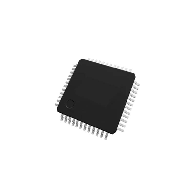
LPC1754FBD80,518

80-Pin LQFP Package


ブランド: NXP SEMICONDUCTORS
製造元部品 #: LPC1754FBD80,518
データシート: LPC1754FBD80,518 データシート (PDF)
パッケージ/ケース: LQFP-80
RoHS ステータス:
在庫状況: 5,792 個、新しいオリジナル
製品の種類: Microcontrollers
Warranty: 1 Year Ovaga Warranty - Find Out More
0
1
*すべての価格は米ドルです
| 数量 | 単価 | 外部価格 |
|---|---|---|
| 1 | $9.232 | $9.232 |
| 10 | $8.098 | $80.980 |
| 30 | $7.408 | $222.240 |
| 100 | $6.828 | $682.800 |
在庫あり: 5,792 PCS
LPC1754FBD80,518 概要
Embedded developers will find the LPC1754FBD80,518 microcontroller to be a versatile platform for a multitude of communication interfaces, including UART, SPI, I2C, and CAN, as well as USB connectivity. This broad spectrum of communication options enables seamless integration with a variety of peripheral devices and networks. Additionally, the microcontroller's abundant timers, PWM channels, analog peripherals, and GPIO pins afford ample flexibility for interfacing with sensors, actuators, and other external hardware components
特徴
- ARM Cortex-M3 processor, running at frequencies of up to 100 MHz
- (LPC1758/56/57/54/52/51) or of up to 120 MHz (LPC1759). A Memory Protection Unit
- (MPU) supporting eight regions is included.
- ARM Cortex-M3 built-in Nested Vectored Interrupt Controller (NVIC).
- Up to 512 kB on-chip flash programming memory. Enhanced flash memory accelerator enables high-speed 120 MHz operation with zero wait states.
- In-System Programming (ISP) and In-Application Programming (IAP) via on-chip bootloader software.
- On-chip SRAM includes:
- ♦ Up to 32 kB of SRAM on the CPU with local code/data bus for high-performance CPU access.
- ♦ Two/one 16 kB SRAM blocks with separate access paths for higher throughput.
- These SRAM blocks may be used for Ethernet (LPC1758 only), USB, and DMA memory, as well as for general purpose CPU instruction and data storage.
- Eight channel General Purpose DMA controller (GPDMA) on the AHB multilayer matrix that can be used with the SSP, I2S-bus, UART, the Analog-to-Digital and Digital-to-Analog converter peripherals, timer match signals, and for memory-to-memory transfers.
- Multilayer AHB matrix interconnect provides a separate bus for each AHB master. AHB masters include the CPU, General Purpose DMA controller, Ethernet MAC (LPC1758 only), and the USB interface. This interconnect provides communication with no arbitration delays.
- Split APB bus allows high throughput with few stalls between the CPU and DMA.
- Serial interfaces:
- ♦ On the LPC1758 only, Ethernet MAC with RMII interface and dedicated DMA controller.
- ♦ USB 2.0 full-speed device/Host/OTG controller with dedicated DMA controller and on-chip PHY for device, Host, and OTG functions. The LPC1752/51 include a USB device controller only.
- ♦ Four UARTs with fractional baud rate generation, internal FIFO, and DMA support. One UART has modem control I/O and RS-485/EIA-485 support, and one UART has IrDA support.
- ♦ CAN 2.0B controller with two (LPC1759/58/56) or one (LPC1754/52/51) channels.
- ♦ SPI controller with synchronous, serial, full duplex communication and programmable data length.
- ♦ Two SSP controllers with FIFO and multi-protocol capabilities. The SSP interfaces can be used with the GPDMA controller.
- ♦ Two I2C-bus interfaces supporting fast mode with a data rate of 400 kbit/s with multiple address recognition and monitor mode.
- ♦ On the LPC1759/58/56 only, I2S (Inter-IC Sound) interface for digital audio input or output, with fractional rate control. The I2S-bus interface can be used with the GPDMA. The I2S-bus interface supports 3-wire and 4-wire data transmit and receive as well as master clock input/output.
- Other peripherals:
- ♦ 52 General Purpose I/O (GPIO) pins with configurable pull-up/down resistors. All GPIOs support a new, configurable open-drain operating mode. The GPIO block is accessed through the AHB multilayer bus for fast access and located in memory such that it supports Cortex-M3 bit banding and use by the General Purpose DMA Controller.
- ♦ 12-bit Analog-to-Digital Converter (ADC) with input multiplexing among six pins, conversion rates up to 200 kHz, and multiple result registers. The 12-bit ADC can be used with the GPDMA controller.
- ♦ On the LPC1759/58/56/54 only, 10-bit Digital-to-Analog Converter (DAC) with dedicated conversion timer and DMA support.
- Four general purpose timers/counters, with a total of three capture inputs and ten compare outputs. Each timer block has an external count input. Specific timer events can be selected to generate DMA requests.
- ♦ One motor control PWM with support for three-phase motor control.
- ♦ Quadrature encoder interface that can monitor one external quadrature encoder.
- ♦ One standard PWM/timer block with external count input.
- ♦ Real-Time Clock (RTC) with a separate power domain and dedicated RTC oscillator. The RTC block includes 20 bytes of battery-powered backup registers.
- ♦ WatchDog Timer (WDT). The WDT can be clocked from the internal RC oscillator, the RTC oscillator, or the APB clock.
- ♦ ARM Cortex-M3 system tick timer, including an external clock input option.
- ♦ Repetitive Interrupt Timer (RIT) provides programmable and repeating timed interrupts.
- ♦ Each peripheral has its own clock divider for further power savings.
仕様
| パラメータ | 価値 | パラメータ | 価値 |
|---|---|---|---|
| Source Content uid | LPC1754FBD80,518 | Rohs Code | Yes |
| Part Life Cycle Code | Active | Ihs Manufacturer | NXP SEMICONDUCTORS |
| Part Package Code | QFP | Package Description | LFQFP, QFP80,.55SQ,20 |
| Pin Count | 80 | Manufacturer Package Code | SOT315-1 |
| Reach Compliance Code | compliant | HTS Code | 8542.31.00.01 |
| Factory Lead Time | 52 Weeks | Samacsys Manufacturer | NXP |
| Has ADC | YES | Address Bus Width | |
| Bit Size | 32 | Clock Frequency-Max | 25 MHz |
| DAC Channels | NO | DMA Channels | YES |
| External Data Bus Width | JESD-30 Code | S-PQFP-G80 | |
| JESD-609 Code | e3 | Length | 12 mm |
| Moisture Sensitivity Level | 2 | Number of I/O Lines | 52 |
| Number of Terminals | 80 | Operating Temperature-Max | 85 °C |
| Operating Temperature-Min | -40 °C | PWM Channels | YES |
| Package Body Material | PLASTIC/EPOXY | Package Code | LFQFP |
| Package Equivalence Code | QFP80,.55SQ,20 | Package Shape | SQUARE |
| Package Style | FLATPACK, LOW PROFILE, FINE PITCH | Peak Reflow Temperature (Cel) | 260 |
| Power Supplies | 3.3 V | Qualification Status | Not Qualified |
| RAM (bytes) | 32768 | ROM (words) | 131072 |
| ROM Programmability | FLASH | Seated Height-Max | 1.6 mm |
| Speed | 100 MHz | Supply Current-Max | 100 mA |
| Supply Voltage-Max | 3.6 V | Supply Voltage-Min | 2.4 V |
| Supply Voltage-Nom | 3.3 V | Surface Mount | YES |
| Technology | CMOS | Temperature Grade | INDUSTRIAL |
| Terminal Finish | TIN | Terminal Form | GULL WING |
| Terminal Pitch | 0.5 mm | Terminal Position | QUAD |
| Time@Peak Reflow Temperature-Max (s) | 30 | Width | 12 mm |
| uPs/uCs/Peripheral ICs Type | MICROCONTROLLER, RISC | Series | LPC17xx |
| Product Status | Active | Programmabe | Not Verified |
| Core Processor | ARM® Cortex®-M3 | Core Size | 32-Bit Single-Core |
| Connectivity | CANbus, I2C, IrDA, Microwire, SPI, SSI, SSP, UART/USART, USB OTG | Peripherals | Brown-out Detect/Reset, DMA, Motor Control PWM, POR, PWM, WDT |
| Number of I/O | 52 | Program Memory Size | 128KB (128K x 8) |
| Program Memory Type | FLASH | RAM Size | 32K x 8 |
| Voltage - Supply (Vcc/Vdd) | 2.4V ~ 3.6V | Data Converters | A/D 6x12b; D/A 1x10b |
| Oscillator Type | Internal | Operating Temperature | -40°C ~ 85°C (TA) |
| Mounting Type | Surface Mount | Package / Case | 80-LQFP |
| Supplier Device Package | 80-LQFP (12x12) |
配送
| 配送タイプ | 配送料 | リードタイム | |
|---|---|---|---|
 |
DHL | $20.00-$40.00 (0.50 KG) | 2-5 日々 |
 |
フェデックス | $20.00-$40.00 (0.50 KG) | 2-5 日々 |
 |
UPS | $20.00-$40.00 (0.50 KG) | 2-5 日々 |
 |
TNT | $20.00-$40.00 (0.50 KG) | 2-5 日々 |
 |
EMS | $20.00-$40.00 (0.50 KG) | 2-5 日々 |
 |
登録された航空便 | $20.00-$40.00 (0.50 KG) | 2-5 日々 |
処理時間:送料は地域や国によって異なります。
支払い
| 支払条件 | ハンドフィー | |
|---|---|---|
 |
電信送金 | 銀行手数料 US$30.00 を請求します。 |
 |
ペイパル | 4.0%のサービス料がかかります。 |
 |
クレジットカード | 3.5%のサービス料がかかります。 |
 |
ウエスタンユニオン | charge US.00 banking fee. |
 |
送金サービス | 銀行手数料は 0.00 米ドルかかります。 |
保証
1.購入した電子部品には365日保証が含まれており、製品の品質を保証します。
2.受け取った商品の一部が完璧な品質ではない場合、当社は責任を持って返金または交換を手配します。 ただし、商品は元の状態のままでなければなりません。
パッキング
-

ステップ1 :製品
-

ステップ2 :真空包装
-

ステップ3 :静電気防止袋
-

ステップ4 :個包装
-

ステップ5 :梱包箱
-

ステップ6 :バーコード配送タグ


すべての製品は静電気防止袋に梱包されます。 ESD 帯電防止保護を備えた状態で出荷されます。
社外の ESD 梱包ラベルには、部品番号、ブランド、数量などの当社の情報が使用されます。
私たちは出荷前にすべての商品を検査し、すべての製品が良好な状態であることを確認し、部品が新しいオリジナルでデータシートと一致していることを確認します。
すべての商品に問題がないことを確認した後、梱包後、安全に梱包し、グローバルエクスプレスで発送します。 優れた耐穿刺性と耐引裂性を示し、シールの完全性も良好です。


私たちは高品質の製品、思いやりのあるサービス、販売後の保証を提供します
-

豊富な商品を取り揃えておりますので、お客様の様々なニーズにお応え致します。
-

最小注文数量は1個からとなります。
-

最低国際配送料は0.00ドルから
-

全商品365日品質保証