


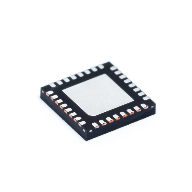
画像は参考用です。製品仕様を参照してください。
注文金額が
$5000LMK04828BISQE/NOPB
Jitter Cleaner IC 3.08GHz 1 64-WFQFN Exposed Pad


LMK04828BISQE/NOPB 概要
Designed as part of the LMK0482x family, the LMK04828BISQE/NOPB combines state-of-the-art technology with advanced features to meet the stringent demands of modern clocking applications. Its ultra-low RMS jitter and noise floor levels set new benchmarks for precision and reliability, guaranteeing high performance in critical systems. The device's extensive range of clock outputs, dual-loop PLL architecture, and integrated functionalities make it a versatile solution for wireless infrastructure, military, aerospace, and other industries. Whether it's video synchronization or data converter clocking, the LMK04828BISQE/NOPB excels in providing exceptional jitter performance and flexibility, making it a top choice for demanding applications
特徴
- JEDEC JESD204B Support
- Ultra-Low RMS Jitter
- 88 fs RMS Jitter (12 kHz to 20 MHz)
- 91 fs RMS Jitter (100 Hz to 20 MHz)
- –162.5 dBc/Hz Noise Floor at 245.76 MHz
- Up to 14 Differential Device Clocks from PLL2
- Up to 7 SYSREF Clocks
- Maximum Clock Output Frequency 3.1 GHz
- LVPECL, LVDS, HSDS, LCPECL Programmable Outputs from PLL2
- Up to 1 Buffered VCXO/Crystal Output from PLL1
- LVPECL, LVDS, 2xLVCMOS Programmable
- Dual Loop PLLatinum™ PLL Architecture
- PLL1
- Up to 3 Redundant Input Clocks
- Automatic and Manual Switch-Over Modes
- Hitless Switching and LOS
- Integrated Low-Noise Crystal Oscillator Circuit
- Holdover Mode When Input Clocks are Lost
- Up to 3 Redundant Input Clocks
- PLL2
- Normalized [1 Hz] PLL Noise Floor of
–227 dBc/Hz - Phase Detector Rate up to 155 MHz
- OSCin Frequency-Doubler
- Two Integrated Low-Noise VCOs
- Normalized [1 Hz] PLL Noise Floor of
- 50% Duty Cycle Output Divides, 1 to 32
(even and odd) - Precision Digital Delay, Dynamically Adjustable
- 25-ps Step Analog Delay
- Multi-Mode: Dual PLL, Single PLL, and Clock Distribution
- Industrial Temperature Range: –40 to 85°C
- Supports 105°C PCB Temperature (Measured at Thermal Pad)
- 3.15-V to 3.45-V Operation
- Package: 64-Pin QFN (9.0 mm × 9.0 mm × 0.8 mm)
仕様
| パラメータ | 価値 | パラメータ | 価値 |
|---|---|---|---|
| Function | Dual-loop PLL | Number of outputs | 15 |
| RMS jitter (fs) | 88 | Output frequency (min) (MHz) | 0.289 |
| Output frequency (max) (MHz) | 3080 | Input type | LVCMOS, LVDS, LVPECL |
| Output type | LVCMOS, LVDS, LVPECL | Supply voltage (min) (V) | 3.15 |
| Supply voltage (max) (V) | 3.45 | Features | JESD204B |
| Rating | Catalog | Operating temperature range (°C) | -40 to 85 |
| Number of input channels | 3 |
配送
| 配送タイプ | 配送料 | リードタイム | |
|---|---|---|---|
 |
DHL | $20.00-$40.00 (0.50 KG) | 2-5 日々 |
 |
フェデックス | $20.00-$40.00 (0.50 KG) | 2-5 日々 |
 |
UPS | $20.00-$40.00 (0.50 KG) | 2-5 日々 |
 |
TNT | $20.00-$40.00 (0.50 KG) | 2-5 日々 |
 |
EMS | $20.00-$40.00 (0.50 KG) | 2-5 日々 |
 |
登録された航空便 | $20.00-$40.00 (0.50 KG) | 2-5 日々 |
処理時間:送料は地域や国によって異なります。
支払い
| 支払条件 | ハンドフィー | |
|---|---|---|
 |
電信送金 | 銀行手数料 US$30.00 を請求します。 |
 |
ペイパル | 4.0%のサービス料がかかります。 |
 |
クレジットカード | 3.5%のサービス料がかかります。 |
 |
ウエスタンユニオン | charge US.00 banking fee. |
 |
送金サービス | 銀行手数料は 0.00 米ドルかかります。 |
保証
1.購入した電子部品には365日保証が含まれており、製品の品質を保証します。
2.受け取った商品の一部が完璧な品質ではない場合、当社は責任を持って返金または交換を手配します。 ただし、商品は元の状態のままでなければなりません。
パッキング
-

ステップ1 :製品
-

ステップ2 :真空包装
-

ステップ3 :静電気防止袋
-

ステップ4 :個包装
-

ステップ5 :梱包箱
-

ステップ6 :バーコード配送タグ


すべての製品は静電気防止袋に梱包されます。 ESD 帯電防止保護を備えた状態で出荷されます。
社外の ESD 梱包ラベルには、部品番号、ブランド、数量などの当社の情報が使用されます。
私たちは出荷前にすべての商品を検査し、すべての製品が良好な状態であることを確認し、部品が新しいオリジナルでデータシートと一致していることを確認します。
すべての商品に問題がないことを確認した後、梱包後、安全に梱包し、グローバルエクスプレスで発送します。 優れた耐穿刺性と耐引裂性を示し、シールの完全性も良好です。


私たちは高品質の製品、思いやりのあるサービス、販売後の保証を提供します
-

豊富な商品を取り揃えておりますので、お客様の様々なニーズにお応え致します。
-

最小注文数量は1個からとなります。
-

最低国際配送料は0.00ドルから
-

全商品365日品質保証


