画像は参考用です。製品仕様を参照してください。
注文金額が
$5000LFXP2-8E-5FTN256C
Low power consumption


ブランド: Lattice Semiconductor Corporation
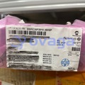
製造元部品 #: LFXP2-8E-5FTN256C
データシート: LFXP2-8E-5FTN256C データシート (PDF)
パッケージ/ケース: 256-LBGA
LFXP2-8E-5FTN256C 概要
Lattice Semiconductor's LFXP2-8E-5FTN256C is a formidable FPGA designed to meet the demands of modern high-performance applications. Featuring 8,192 LUTs, 193 user I/Os, and 238 I/Os, this device offers a comprehensive set of resources for complex design requirements. With a 256-pin FBGA package, the FPGA ensures secure and reliable connectivity, making it suitable for a diverse range of industrial and commercial applications. Operating at a 1.2V core voltage and supporting a variety of I/O standards, including LVCMOS, LVTTL, and LVDS, the LFXP2-8E-5FTN256C provides flexibility and compatibility with different interface needs. Moreover, the inclusion of PLLs, block RAM, and dedicated multipliers enhances its signal processing and data manipulation capabilities, catering to the needs of advanced applications. Programmed using the intuitive Lattice Diamond design software, the FPGA offers a seamless and efficient development process, ensuring quick integration into various systems. With its advanced features and robust construction, the LFXP2-8E-5FTN256C stands as a reliable and powerful choice for engineers and developers seeking a high-performance FPGA solution
特徴
- Fully supports PowerPC™ 60x bus protocol, include PowerPC 603, 604, 740, 750 and 8260.
- Supports up to eight PowerPC bus masters with unlimited slave device support.
- Supports two outstanding bus accesses.
- Supports address only transfer and address bus retry.
- Independent address bus and data bus tenure with separate bus grant and data bus grant.
- Option for fixed priority assignment or rotating priority scheme.
- Designed for ASIC or programmable logic device implementations in various system environments.
- Fully static design with edge triggered flip-flops.
- Optimized for ispXPGA product family.
仕様
| パラメータ | 価値 | パラメータ | 価値 |
|---|---|---|---|
| Series | XP2 | Package | Tray |
| Product Status | Active | Programmabe | Not Verified |
| Number of LABs/CLBs | 1000 | Number of Logic Elements/Cells | 8000 |
| Total RAM Bits | 226304 | Number of I/O | 201 |
| Voltage - Supply | 1.14V ~ 1.26V | Mounting Type | Surface Mount |
| Operating Temperature | 0°C ~ 85°C (TJ) | Package / Case | 256-LBGA |
| Supplier Device Package | 256-FTBGA (17x17) |
配送
| 配送タイプ | 配送料 | リードタイム | |
|---|---|---|---|
 |
DHL | $20.00-$40.00 (0.50 KG) | 2-5 日々 |
 |
フェデックス | $20.00-$40.00 (0.50 KG) | 2-5 日々 |
 |
UPS | $20.00-$40.00 (0.50 KG) | 2-5 日々 |
 |
TNT | $20.00-$40.00 (0.50 KG) | 2-5 日々 |
 |
EMS | $20.00-$40.00 (0.50 KG) | 2-5 日々 |
 |
登録された航空便 | $20.00-$40.00 (0.50 KG) | 2-5 日々 |
処理時間:送料は地域や国によって異なります。
支払い
| 支払条件 | ハンドフィー | |
|---|---|---|
 |
電信送金 | 銀行手数料 US$30.00 を請求します。 |
 |
ペイパル | 4.0%のサービス料がかかります。 |
 |
クレジットカード | 3.5%のサービス料がかかります。 |
 |
ウエスタンユニオン | charge US.00 banking fee. |
 |
送金サービス | 銀行手数料は 0.00 米ドルかかります。 |
保証
1.購入した電子部品には365日保証が含まれており、製品の品質を保証します。
2.受け取った商品の一部が完璧な品質ではない場合、当社は責任を持って返金または交換を手配します。 ただし、商品は元の状態のままでなければなりません。
パッキング
-

ステップ1 :製品
-

ステップ2 :真空包装
-

ステップ3 :静電気防止袋
-

ステップ4 :個包装
-

ステップ5 :梱包箱
-

ステップ6 :バーコード配送タグ


すべての製品は静電気防止袋に梱包されます。 ESD 帯電防止保護を備えた状態で出荷されます。
社外の ESD 梱包ラベルには、部品番号、ブランド、数量などの当社の情報が使用されます。
私たちは出荷前にすべての商品を検査し、すべての製品が良好な状態であることを確認し、部品が新しいオリジナルでデータシートと一致していることを確認します。
すべての商品に問題がないことを確認した後、梱包後、安全に梱包し、グローバルエクスプレスで発送します。 優れた耐穿刺性と耐引裂性を示し、シールの完全性も良好です。


パーツポイント
-
The LFXP2-8E-5FTN256C is a low-power, low-cost FPGA chip from Lattice Semiconductor, featuring 2,520 LUTs, 39 kbits of embedded memory, and 16 multibit arithmetic blocks. It offers high reliability and performance for various applications such as industrial control, automotive, and communications. With its small form factor and low power consumption, it is suitable for battery-operated and compact devices.
-
Equivalent
The equivalent products of LFXP2-8E-5FTN256C chip are the following: LFE2-6E, LFE2-15E, and LFE2-35E FPGAs from Lattice Semiconductor. These chips have similar features and performance characteristics, making them suitable replacements for the LFXP2-8E-5FTN256C chip. -
Features
- Lattice XP2 series FPGA - 8K LUTs - 200 MHz - Flash technology - 144 I/O pins - 32 Kbit embedded block RAM - 256-ball fine pitch BGA package - Low power consumption - Programming and reconfiguration through JTAG - High reliability and security features -
Pinout
The LFXP2-8E-5FTN256C is a Lattice FPGA with 256-pin in a 14x14 mm package. It has 8,000 LUTs, 18 I/O banks, 2.5 Mbit embedded memory, and PLLs. The pins are used for power, ground, configuration, I/O, clock input, and other functions to support programmable logic design. -
Manufacturer
The LFXP2-8E-5FTN256C is manufactured by Lattice Semiconductor Corporation. Lattice Semiconductor Corporation is a global semiconductor company that designs and produces programmable logic devices and related software. They specialize in low-power, small form-factor programmable logic devices for a variety of applications in the consumer, communications, and industrial markets. -
Application Field
The LFXP2-8E-5FTN256C is commonly used in industrial control systems, communication equipment, automotive electronics, and consumer electronics. It is ideal for applications that require low power consumption, high performance, and integration of multiple functions in a compact package. Its flexibility and programmability make it suitable for a wide range of embedded applications. -
Package
The LFXP2-8E-5FTN256C chip is a Field Programmable Gate Array (FPGA) packaged in a 256-pin FineLine BGA form. It has a package size of 17x17mm.


私たちは高品質の製品、思いやりのあるサービス、販売後の保証を提供します
-

豊富な商品を取り揃えておりますので、お客様の様々なニーズにお応え致します。
-

最小注文数量は1個からとなります。
-

最低国際配送料は0.00ドルから
-

全商品365日品質保証