画像は参考用です。製品仕様を参照してください。
注文金額が
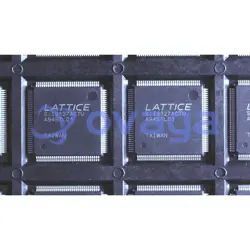
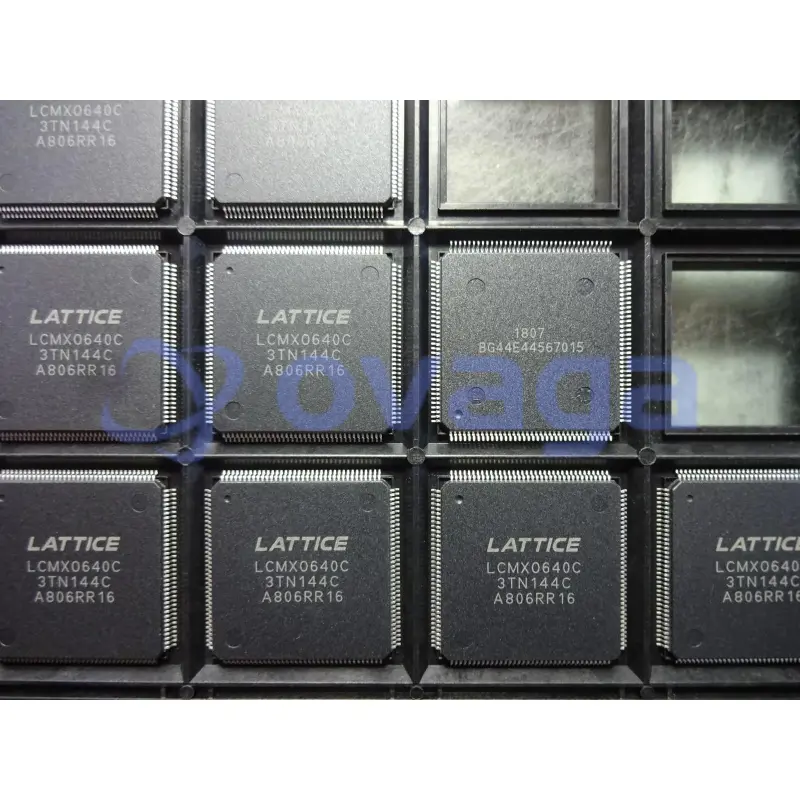
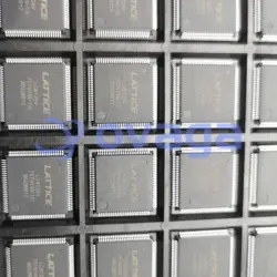
$5000LATTICE LCMXO640C-3TN144C
Programmable FPGA with 640 LUTs and 113 I/O


LCMXO640C-3TN144C 概要
When it comes to programmability and flexibility, the LCMXO640C-3TN144C FPGA stands out with its field programmable gate array technology. This FPGA offers engineers the ability to customize their logic functions according to specific application requirements. With the 640 LUTs onboard, designers have ample resources to implement complex algorithms and logic operations efficiently
特徴
- Non-volatile, Infinitely Reconfigurable
- Instant-on – powers up in microseconds
- Single chip, no external configuration memory
- required
- Excellent design security, no bit stream to
- intercept
- Reconfigure SRAM based logic in milliseconds
- SRAM and non-volatile memory programmable
- through JTAG port
- Supports background programming of
- non-volatile memory
- Sleep Mode
- Allows up to 100x static current reduction
- TransFR™ Reconfiguration (TFR)
- In-field logic update while system operates
- High I/O to Logic Density
- 256 to 2280 LUT4s
- 73 to 271 I/Os with extensive package options
- Density migration supported
- Lead free/RoHS compliant packaging
- Embedded and Distributed Memory
- Up to 27.6 Kbits sysMEM™ Embedded Block
- RAM
- Up to 7.5 Kbits distributed RAM
- Dedicated FIFO control logic
- Flexible I/O Buffer
- Programmable sysIO™ buffer supports wide
- range of interfaces:
- − LVCMOS 3.3/2.5/1.8/1.5/1.2
- − LVTTL
- − PCI
- − LVDS, Bus-LVDS, LVPECL, RSDS
- sysCLOCK™ PLLs
- Up to two analog PLLs per device
- Clock multiply, divide, and phase shifting
- System Level Support
- IEEE Standard 1149.1 Boundary Scan
- Onboard oscillator
- Devices operate with 3.3V, 2.5V, 1.8V or 1.2V
- power supply
- IEEE 1532 compliant in-system programming

仕様
| パラメータ | 価値 | パラメータ | 価値 |
|---|---|---|---|
| Product Category | FPGA - Field Programmable Gate Array | RoHS | Details |
| Series | LCMXO640C | Number of Logic Elements | 640 LE |
| Adaptive Logic Modules - ALMs | 320 ALM | Embedded Memory | 0 bit |
| Number of I/Os | 113 I/O | Supply Voltage - Min | 1.71 V |
| Supply Voltage - Max | 3.465 V | Minimum Operating Temperature | 0 C |
| Maximum Operating Temperature | + 85 C | Mounting Style | SMD/SMT |
| Package / Case | CSBGA-144 | Brand | Lattice |
| Distributed RAM | 6.1 kbit | Height | 1.4 mm |
| Length | 20 mm | Maximum Operating Frequency | 500 MHz |
| Moisture Sensitive | Yes | Number of Logic Array Blocks - LABs | 80 LAB |
| Operating Supply Current | 17 mA | Operating Supply Voltage | 1.8 V/2.5 V/3.3 V |
| Product Type | FPGA - Field Programmable Gate Array | Factory Pack Quantity | 60 |
| Subcategory | Programmable Logic ICs | Total Memory | 6.1 kbit |
| Width | 20 mm |
配送
| 配送タイプ | 配送料 | リードタイム | |
|---|---|---|---|
 |
DHL | $20.00-$40.00 (0.50 KG) | 2-5 日々 |
 |
フェデックス | $20.00-$40.00 (0.50 KG) | 2-5 日々 |
 |
UPS | $20.00-$40.00 (0.50 KG) | 2-5 日々 |
 |
TNT | $20.00-$40.00 (0.50 KG) | 2-5 日々 |
 |
EMS | $20.00-$40.00 (0.50 KG) | 2-5 日々 |
 |
登録された航空便 | $20.00-$40.00 (0.50 KG) | 2-5 日々 |
処理時間:送料は地域や国によって異なります。
支払い
| 支払条件 | ハンドフィー | |
|---|---|---|
 |
電信送金 | 銀行手数料 US$30.00 を請求します。 |
 |
ペイパル | 4.0%のサービス料がかかります。 |
 |
クレジットカード | 3.5%のサービス料がかかります。 |
 |
ウエスタンユニオン | charge US.00 banking fee. |
 |
送金サービス | 銀行手数料は 0.00 米ドルかかります。 |
保証
1.購入した電子部品には365日保証が含まれており、製品の品質を保証します。
2.受け取った商品の一部が完璧な品質ではない場合、当社は責任を持って返金または交換を手配します。 ただし、商品は元の状態のままでなければなりません。
パッキング
-

ステップ1 :製品
-

ステップ2 :真空包装
-

ステップ3 :静電気防止袋
-

ステップ4 :個包装
-

ステップ5 :梱包箱
-

ステップ6 :バーコード配送タグ


すべての製品は静電気防止袋に梱包されます。 ESD 帯電防止保護を備えた状態で出荷されます。
社外の ESD 梱包ラベルには、部品番号、ブランド、数量などの当社の情報が使用されます。
私たちは出荷前にすべての商品を検査し、すべての製品が良好な状態であることを確認し、部品が新しいオリジナルでデータシートと一致していることを確認します。
すべての商品に問題がないことを確認した後、梱包後、安全に梱包し、グローバルエクスプレスで発送します。 優れた耐穿刺性と耐引裂性を示し、シールの完全性も良好です。


パーツポイント
-
The LCMXO640C-3TN144C is a programmable logic device (PLD) chip manufactured by Lattice Semiconductor. It belongs to the Lattice XO2 family of FPGAs and has 640 Look-Up Tables (LUTs) and 640 logical registers. With a density of 640 LUTs, this chip offers a cost-effective and low-power solution for a variety of applications such as consumer electronics, industrial automation, and communication devices.
-
Features
LCMXO640C-3TN144C is a low-power, non-volatile PLD (Programmable Logic Device) with a capacity of 640 Look-Up Tables (LUTs) and 32640 bits of RAM. It operates with a supply voltage of 3.3V and offers 144-pin TQFP packaging. Additionally, it features an internal oscillator and programmable routing to cater to various digital designs. -
Pinout
The LCMXO640C-3TN144C is a Field-Programmable Gate Array (FPGA) with a pin count of 144. It functions as a programmable logic device that can be configured to perform various digital functions. -
Manufacturer
The manufacturer of the LCMXO640C-3TN144C is Lattice Semiconductor Corporation. It is a semiconductor company that specializes in the design and manufacture of programmable logic devices, including field-programmable gate arrays (FPGAs) and complex programmable logic devices (CPLDs). -
Application Field
The LCMXO640C-3TN144C can be used in various application areas such as portable consumer electronics, industrial automation, automotive systems, and communication devices. -
Package
The LCMXO640C-3TN144C chip has a package type of TQFP (Thin Quad Flat Package), a form of leaded surface mount, and a size of 14 x 14 mm.


私たちは高品質の製品、思いやりのあるサービス、販売後の保証を提供します
-

豊富な商品を取り揃えておりますので、お客様の様々なニーズにお応え致します。
-

最小注文数量は1個からとなります。
-

最低国際配送料は0.00ドルから
-

全商品365日品質保証