


画像は参考用です。製品仕様を参照してください。
注文金額が
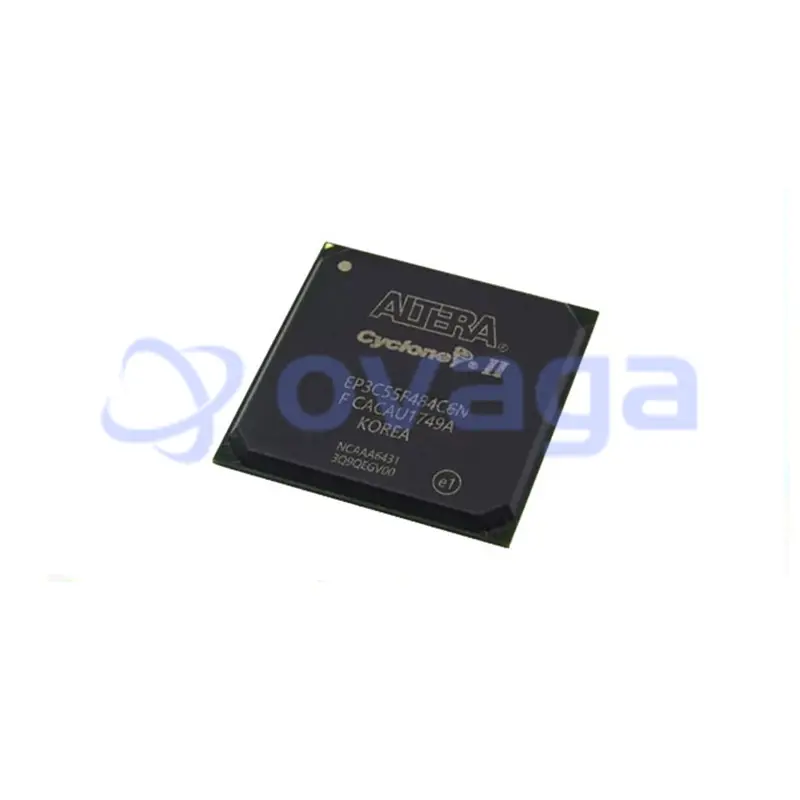
$5000Altera EP3C55F484C6N
FPGA Cyclone® III Family 55856 Cells 500MHz 65nm Technology 1.2V 484-Pin FBGA


ブランド: Altera Corporation (Intel)
製造元部品 #: EP3C55F484C6N
データシート: EP3C55F484C6N Datasheet (PDF)
パッケージ/ケース: FBGA-484
EP3C55F484C6N 概要
Cyclone® III Field Programmable Gate Array (FPGA) IC 327 2396160 55856 484-BGA
特徴
- FPGA density: 55,000 logic elements (LEs)
- Total RAM: 1,890 kilobits
- Maximum number of I/O pins: 347
- Maximum user I/O pins: 239
- Clock management: Phase-Locked Loops (PLLs), Clock Multiplication, and Clock Phase Adjustment
- Embedded memory blocks: M4K blocks for storing configuration data or user-defined data
- Configuration scheme: Active Serial (AS) or Joint Test Action Group (JTAG)
応用
- Industrial control systems
- Communications and networking equipment
- Video and image processing
- Aerospace and defense systems
- Automotive electronics
- Medical equipment
仕様
| パラメータ | 価値 | パラメータ | 価値 |
|---|---|---|---|
| feature-family-name | Cyclone® III | feature-process-technology | 65nm |
| feature-maximum-number-of-user-i-os | 327 | feature-number-of-registers | |
| feature-device-logic-cells | 55856 | feature-device-system-gates | |
| feature-number-of-multipliers | 156 (18x18) | feature-program-memory-type | SRAM |
| feature-ram-bits-kbit | 2340 | feature-total-number-of-block-ram | 260 |
| feature-ethernet-macs | feature-supported-ip-core | Viterbi Compiler, Low-Speed/Hybrid Serial Decoder|V1 ColdFire|SpeedView Enabled JPEG Encoder (SVE-JPEG-E)|10 Gigabit Ethernet MAC|32/64-bit PCI-X bus Master/Target interface Core, 66/100/133Mhz | |
| feature-supported-ip-core-manufacture | Altera/Freescale/CAST, Inc/MorethanIP/PLDA | feature-maximum-number-of-serdes-channels | |
| feature-device-logic-units | 55856 | feature-device-number-of-dlls-plls | 4 |
| feature-transceiver-blocks | feature-transceiver-speed-gbps | ||
| feature-dedicated-dsp | feature-pci-blocks | ||
| feature-programmability | No | feature-maximum-internal-frequency-mhz | 500 |
| feature-speed-grade | 6 | feature-giga-multiply-accumulates-per-second | |
| feature-differential-i-o-standards-supported | LVPECL|LVDS|HSTL-18|HSTL-15|HSTL-12|SSTL-2|SSTL-18|RSDS | feature-single-ended-i-o-standards-supported | LVTTL|LVCMOS|PCI|PCI-X|SSTL|HSTL |
| feature-external-memory-interface | DDR2 SDRAM|QDRII+SRAM | feature-minimum-operating-supply-voltage-v | 1.15 |
| feature-maximum-operating-supply-voltage-v | 1.25 | feature-packaging | |
| feature-rohs | feature-rad-hard | ||
| feature-pin-count | 484 | feature-supplier-package | FBGA |
| feature-standard-package-name1 | BGA | feature-cecc-qualified | No |
| feature-esd-protection | feature-escc-qualified | ||
| feature-military | No | feature-aec-qualified | No |
| feature-aec-qualified-number | feature-auto-motive | No | |
| feature-p-pap | No | feature-eccn-code | 3A991 |
| feature-svhc | Yes |
配送
| 配送タイプ | 配送料 | リードタイム | |
|---|---|---|---|
 |
DHL | $20.00-$40.00 (0.50 KG) | 2-5 日々 |
 |
フェデックス | $20.00-$40.00 (0.50 KG) | 2-5 日々 |
 |
UPS | $20.00-$40.00 (0.50 KG) | 2-5 日々 |
 |
TNT | $20.00-$40.00 (0.50 KG) | 2-5 日々 |
 |
EMS | $20.00-$40.00 (0.50 KG) | 2-5 日々 |
 |
登録された航空便 | $20.00-$40.00 (0.50 KG) | 2-5 日々 |
処理時間:送料は地域や国によって異なります。
支払い
| 支払条件 | ハンドフィー | |
|---|---|---|
 |
電信送金 | 銀行手数料 US$30.00 を請求します。 |
 |
ペイパル | 4.0%のサービス料がかかります。 |
 |
クレジットカード | 3.5%のサービス料がかかります。 |
 |
ウエスタンユニオン | charge US.00 banking fee. |
 |
送金サービス | 銀行手数料は 0.00 米ドルかかります。 |
保証
1.購入した電子部品には365日保証が含まれており、製品の品質を保証します。
2.受け取った商品の一部が完璧な品質ではない場合、当社は責任を持って返金または交換を手配します。 ただし、商品は元の状態のままでなければなりません。
パッキング
-

ステップ1 :製品
-

ステップ2 :真空包装
-

ステップ3 :静電気防止袋
-

ステップ4 :個包装
-

ステップ5 :梱包箱
-

ステップ6 :バーコード配送タグ


すべての製品は静電気防止袋に梱包されます。 ESD 帯電防止保護を備えた状態で出荷されます。
社外の ESD 梱包ラベルには、部品番号、ブランド、数量などの当社の情報が使用されます。
私たちは出荷前にすべての商品を検査し、すべての製品が良好な状態であることを確認し、部品が新しいオリジナルでデータシートと一致していることを確認します。
すべての商品に問題がないことを確認した後、梱包後、安全に梱包し、グローバルエクスプレスで発送します。 優れた耐穿刺性と耐引裂性を示し、シールの完全性も良好です。


パーツポイント
-
The EP3C55F484C6N is a programmable logic device (PLD) from Altera (now Intel) that is part of the Cyclone III family. It features 55,000 logic elements, 6 Mbit of RAM, and 484 user I/O pins. This chip is commonly used for a wide range of applications including telecommunications, consumer electronics, and industrial automation.
-
Equivalent
Some equivalent products of the EP3C55F484C6N chip include Altera Cyclone III EP3C55 F484C chip, EP3C55Q124 EP3C55Q124 F484C6N FPGA, and Altera Cyclone III EP3C55 AG1152C chip. These chips offer similar features and functionality to the EP3C55F484C6N chip. -
Features
- Low power consumption - High logic density - Embedded memory blocks - Low-cost and high performance - MultiVolt I/O standard support - Built-in security features - Integrated phase-locked loop (PLL) - Flexible and configurable I/O options -
Pinout
The EP3C55F484C6N is a 484-pin FPGA (Field-Programmable Gate Array) with 55,000 logic elements and 484 user I/O pins. It is used for creating custom digital circuits. The functions of the pins can be configured by the user to perform various functions such as input, output, or as part of the logic circuit. -
Manufacturer
The EP3C55F484C6N is manufactured by Altera Corporation, which is a leading provider of programmable logic devices and related technologies. Altera is a semiconductor company that specializes in designing and manufacturing field-programmable gate arrays (FPGAs) and complex programmable logic devices (CPLDs) for a wide range of applications in various industries. -
Application Field
The EP3C55F484C6N is commonly used in applications such as automation, communication, automotive, and industrial control systems. It is also suitable for consumer electronics, medical devices, and military applications that require high performance, low power consumption, and flexibility in design. -
Package
The EP3C55F484C6N chip comes in a plastic package with a ball grid array form. It has a size of 23mm x 23mm, with a 484-pin count.


データシート PDF
私たちは高品質の製品、思いやりのあるサービス、販売後の保証を提供します
-

豊富な商品を取り揃えておりますので、お客様の様々なニーズにお応え致します。
-

最小注文数量は1個からとなります。
-

最低国際配送料は0.00ドルから
-

全商品365日品質保証


