


画像は参考用です。製品仕様を参照してください。
注文金額が
$5000Altera EP2S30F484I4N
694 CLBs, 717MHz


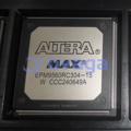
ブランド: Altera Corporation (Intel)
製造元部品 #: EP2S30F484I4N
データシート: EP2S30F484I4N Datasheet (PDF)
パッケージ/ケース: FBGA-484
EP2S30F484I4N 概要
The FPGA also supports a range of high-speed interfaces, including SERDES, LVDS, and DDR SDRAM controllers. This enables seamless integration with external devices and ensures reliable data transfer across different systems
特徴
- It has a maximum of 31,680 logic elements (LEs) and 1,330 Kbits of embedded memory.
- It operates with a maximum frequency of 500 MHz and has 720 user I/O pins.
- It supports multiple I/O standards, including LVDS, PCI Express, and DDR3.
応用
- EP2S30F484I4N is commonly used in high-performance computing applications, including data centers, network infrastructure, and scientific research.
- It can also be used in digital signal processing, video processing, and other applications that require high-speed data transfer and real-time processing.
 Inventory")
仕様
| パラメータ | 価値 | パラメータ | 価値 |
|---|---|---|---|
| feature-family-name | Stratix® II | feature-process-technology | 90nm |
| feature-maximum-number-of-user-i-os | 342 | feature-number-of-registers | |
| feature-device-logic-cells | 33880 | feature-device-system-gates | |
| feature-number-of-multipliers | 64 (18x18) | feature-program-memory-type | SRAM |
| feature-ram-bits-kbit | 1337.6 | feature-total-number-of-block-ram | 1+144+202 |
| feature-ethernet-macs | feature-supported-ip-core | 32/64-bit PCI-X bus Master/Target interface Core, 66/100/133Mhz|PowerPC/SH/1960 System Controller|RapidIO to AXI Bridge Controller (RAB)|Viterbi Compiler, High-Speed Parallel Decoder | |
| feature-supported-ip-core-manufacture | Altera/CAST, Inc/Barco Silex/Mobiveil, Inc/Eureka Technology Inc/PLDA | feature-maximum-number-of-serdes-channels | |
| feature-device-logic-units | 33880 | feature-device-number-of-dlls-plls | 6 |
| feature-transceiver-blocks | feature-transceiver-speed-gbps | ||
| feature-dedicated-dsp | 16 | feature-pci-blocks | |
| feature-programmability | No | feature-maximum-internal-frequency-mhz | 711.24 |
| feature-speed-grade | 4 | feature-giga-multiply-accumulates-per-second | 16.8 |
| feature-differential-i-o-standards-supported | LVDS|LVPECL | feature-single-ended-i-o-standards-supported | HSTL|SSTL|CMOS|LVTTL |
| feature-external-memory-interface | QDRII+SRAM|RLDRAM II|DDR2 SDRAM|DDR SDRAM | feature-minimum-operating-supply-voltage-v | 1.15 |
| feature-maximum-operating-supply-voltage-v | 1.25 | feature-packaging | |
| feature-rohs | feature-rad-hard | ||
| feature-pin-count | 484 | feature-supplier-package | FC-FBGA |
| feature-standard-package-name1 | BGA | feature-cecc-qualified | No |
| feature-esd-protection | feature-escc-qualified | ||
| feature-military | No | feature-aec-qualified | No |
| feature-aec-qualified-number | feature-auto-motive | No | |
| feature-p-pap | No | feature-eccn-code | 3A991 |
| feature-svhc | Yes |
配送
| 配送タイプ | 配送料 | リードタイム | |
|---|---|---|---|
 |
DHL | $20.00-$40.00 (0.50 KG) | 2-5 日々 |
 |
フェデックス | $20.00-$40.00 (0.50 KG) | 2-5 日々 |
 |
UPS | $20.00-$40.00 (0.50 KG) | 2-5 日々 |
 |
TNT | $20.00-$40.00 (0.50 KG) | 2-5 日々 |
 |
EMS | $20.00-$40.00 (0.50 KG) | 2-5 日々 |
 |
登録された航空便 | $20.00-$40.00 (0.50 KG) | 2-5 日々 |
処理時間:送料は地域や国によって異なります。
支払い
| 支払条件 | ハンドフィー | |
|---|---|---|
 |
電信送金 | 銀行手数料 US$30.00 を請求します。 |
 |
ペイパル | 4.0%のサービス料がかかります。 |
 |
クレジットカード | 3.5%のサービス料がかかります。 |
 |
ウエスタンユニオン | charge US.00 banking fee. |
 |
送金サービス | 銀行手数料は 0.00 米ドルかかります。 |
保証
1.購入した電子部品には365日保証が含まれており、製品の品質を保証します。
2.受け取った商品の一部が完璧な品質ではない場合、当社は責任を持って返金または交換を手配します。 ただし、商品は元の状態のままでなければなりません。
パッキング
-

ステップ1 :製品
-

ステップ2 :真空包装
-

ステップ3 :静電気防止袋
-

ステップ4 :個包装
-

ステップ5 :梱包箱
-

ステップ6 :バーコード配送タグ


すべての製品は静電気防止袋に梱包されます。 ESD 帯電防止保護を備えた状態で出荷されます。
社外の ESD 梱包ラベルには、部品番号、ブランド、数量などの当社の情報が使用されます。
私たちは出荷前にすべての商品を検査し、すべての製品が良好な状態であることを確認し、部品が新しいオリジナルでデータシートと一致していることを確認します。
すべての商品に問題がないことを確認した後、梱包後、安全に梱包し、グローバルエクスプレスで発送します。 優れた耐穿刺性と耐引裂性を示し、シールの完全性も良好です。


同等部品
のために EP2S30F484I4N コンポーネントの場合は、これらの交換部品および代替部品を検討してください:
部品番号
ブランド
パッケージ
説明
部品番号 : EP2S30F484C5N
ブランド :
パッケージ : FBGA-484
説明 : Stratix® II Family 33880 Cells 609.76MHz 90nm Technology 1.2V
部品番号 : EP2S30F484I5N
ブランド :
パッケージ :
説明 :
部品番号 : EP2S30F484I5LN
ブランド :
パッケージ :
説明 :
部品番号 : EP2S30F484I6N
ブランド :
パッケージ :
説明 :
部品番号 : EP2S30F484I7N
ブランド :
パッケージ :
説明 :
部品番号 : EP2S30F484I7LN
ブランド :
パッケージ :
説明 :
部品番号 : EP2S30F484I8N
ブランド :
パッケージ :
説明 :
部品番号 : EP2S30F484I8LN
ブランド :
パッケージ :
説明 :
パーツポイント
-
The EP2S30F484I4N chip is a field-programmable gate array (FPGA) manufactured by Altera. It belongs to the Stratix II family and offers a balance between cost and performance. With 30,000 logic elements and high-speed I/O interfaces, it is designed for a wide range of applications in communications, industrial automation, and other fields. The chip provides flexibility and scalability, allowing for the implementation of complex digital systems with customizable functionality.
-
Equivalent
Some equivalent products to the EP2S30F484I4N chip include the Xilinx Virtex-II Pro XC2VP30 and the Altera Stratix II EP2S30. -
Features
The main features of EP2S30F484I4N are: - It is a Field-Programmable Gate Array (FPGA) device. - It has a capacity of 30,608 logic elements. - It has a maximum of 540 user I/O pins. - It operates at a speed of up to 166 MHz. - It supports various communication protocols, such as PCI Express, Ethernet, and USB. -
Pinout
The EP2S30F484I4N is an FPGA device with a pin count of 484. It is used for high-performance applications and offers various functions, including programmable logic elements, embedded memory, logic array blocks, I/O elements, and high-speed interfaces. -
Manufacturer
The manufacturer of the EP2S30F484I4N is Altera Corporation. Altera Corporation is a semiconductor company specializing in programmable logic devices, software, and intellectual property. The company is known for its FPGA (field-programmable gate array) technology, which allows customers to customize chips according to their specific design requirements. -
Application Field
The EP2S30F484I4N is commonly used in industrial automation, communication equipment, medical devices, and aerospace applications. It is suitable for tasks that require high-performance processing, low power consumption, and reliable operation in demanding environments. -
Package
The EP2S30F484I4N chip is packaged in a 484-pin FineLine BGA (Ball Grid Array) package, featuring a 23 mm x 23 mm size.


データシート PDF
私たちは高品質の製品、思いやりのあるサービス、販売後の保証を提供します
-

豊富な商品を取り揃えておりますので、お客様の様々なニーズにお応え致します。
-

最小注文数量は1個からとなります。
-

最低国際配送料は0.00ドルから
-

全商品365日品質保証


