画像は参考用です。製品仕様を参照してください。
注文金額が
$5000EP2S180F1020C3
With its Field Programmable Gate Array technology, the EP2S180F1020C3 offers customizable solutions for complex designs


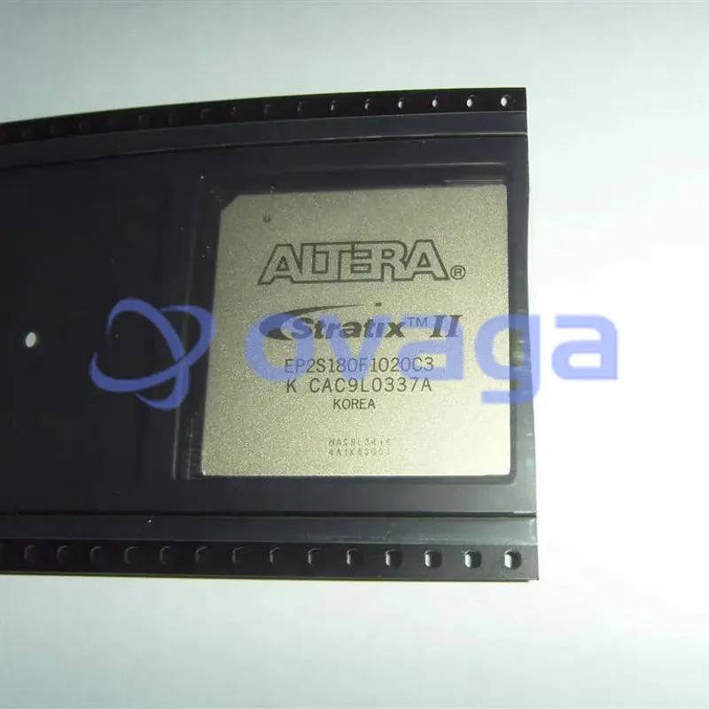
EP2S180F1020C3 概要
Boasting a 180,000 logic element capacity and a C3 speed grade, the EP2S180F1020C3 is a formidable Altera Stratix II FPGA designed for high-performance processing. With 1,020 pins and a wide range of I/O options, this FPGA is equipped to handle complex logic functions, high-speed data processing, and real-time signal processing across various industries. Its support for embedded memory blocks, high-speed transceivers, and flexible routing resources ensures that it can meet the demanding requirements of modern applications
特徴
- The Stratix II family offers the following
- features:
- 15,600 to 179,400 equivalent LEs; see Table 1–1
- New and innovative adaptive logic module (ALM), the basic building block of the Stratix II architecture, maximizes performance and resource usage efficiency
- Up to 9,383,040 RAM bits (1,172,880 bytes) available without reducing logic resources
- TriMatrix memory consisting of three RAM block sizes to implement true dual-port memory and first-in first-out (FIFO) buffers
- High-speed DSP blocks provide dedicated implementation of multipliers (at up to 450 MHz), multiply-accumulate functions, and finite impulse response (FIR) filters
- Up to 16 global clocks with 24 clocking resources per device region
- Clock control blocks support dynamic clock network enable/disable, which allows clock networks to power down to reduce power consumption in user mode
- Up to 12 PLLs (four enhanced PLLs and eight fast PLLs) per device provide spread spectrum, programmable bandwidth, clock switchover, real-time PLL reconfiguration, and advanced multiplication and phase shifting
- Support for numerous single-ended and differential I/O standards
- High-speed differential I/O support with DPA circuitry for 1-Gbps performance
- Support for high-speed networking and communications bus standards including Parallel RapidIO, SPI-4 Phase 2 (POS-PHY Level 4), HyperTransport™ technology, and SFI-4
- Support for high-speed external memory, including DDR and DDR2 SDRAM, RLDRAM II, QDR II SRAM, and SDR SDRAM
- Support for multiple intellectual property megafunctions from Altera MegaCore® functions and Altera Megafunction Partners Program (AMPPSM) megafunctions
- Support for design security using configuration bitstream encryption
- Support for remote configuration updates
仕様
| パラメータ | 価値 | パラメータ | 価値 |
|---|---|---|---|
| Pbfree Code | No | Rohs Code | No |
| Part Life Cycle Code | Transferred | Ihs Manufacturer | ALTERA CORP |
| Part Package Code | BGA | Package Description | 33 X 33 MM, 1 MM PITCH, FBGA-1020 |
| Pin Count | 1020 | Reach Compliance Code | not_compliant |
| HTS Code | 8542.39.00.01 | Clock Frequency-Max | 717 MHz |
| Combinatorial Delay of a CLB-Max | 4.672 ns | JESD-30 Code | S-PBGA-B1020 |
| JESD-609 Code | e0 | Length | 33 mm |
| Moisture Sensitivity Level | 4 | Number of CLBs | 71760 |
| Number of Inputs | 742 | Number of Logic Cells | 179400 |
| Number of Outputs | 734 | Number of Terminals | 1020 |
| Operating Temperature-Max | 85 °C | Operating Temperature-Min | |
| Organization | 71760 CLBS | Package Body Material | PLASTIC/EPOXY |
| Package Code | BGA | Package Equivalence Code | BGA1020,32X32,40 |
| Package Shape | SQUARE | Package Style | GRID ARRAY |
| Peak Reflow Temperature (Cel) | 220 | Power Supplies | 1.2,1.5/3.3,3.3 V |
| Programmable Logic Type | FIELD PROGRAMMABLE GATE ARRAY | Qualification Status | Not Qualified |
| Seated Height-Max | 3.5 mm | Supply Voltage-Max | 1.25 V |
| Supply Voltage-Min | 1.15 V | Supply Voltage-Nom | 1.2 V |
| Surface Mount | YES | Technology | CMOS |
| Temperature Grade | OTHER | Terminal Finish | TIN LEAD |
| Terminal Form | BALL | Terminal Pitch | 1 mm |
| Terminal Position | BOTTOM | Time@Peak Reflow Temperature-Max (s) | 20 |
| Width | 33 mm |
配送
| 配送タイプ | 配送料 | リードタイム | |
|---|---|---|---|
 |
DHL | $20.00-$40.00 (0.50 KG) | 2-5 日々 |
 |
フェデックス | $20.00-$40.00 (0.50 KG) | 2-5 日々 |
 |
UPS | $20.00-$40.00 (0.50 KG) | 2-5 日々 |
 |
TNT | $20.00-$40.00 (0.50 KG) | 2-5 日々 |
 |
EMS | $20.00-$40.00 (0.50 KG) | 2-5 日々 |
 |
登録された航空便 | $20.00-$40.00 (0.50 KG) | 2-5 日々 |
処理時間:送料は地域や国によって異なります。
支払い
| 支払条件 | ハンドフィー | |
|---|---|---|
 |
電信送金 | 銀行手数料 US$30.00 を請求します。 |
 |
ペイパル | 4.0%のサービス料がかかります。 |
 |
クレジットカード | 3.5%のサービス料がかかります。 |
 |
ウエスタンユニオン | charge US.00 banking fee. |
 |
送金サービス | 銀行手数料は 0.00 米ドルかかります。 |
保証
1.購入した電子部品には365日保証が含まれており、製品の品質を保証します。
2.受け取った商品の一部が完璧な品質ではない場合、当社は責任を持って返金または交換を手配します。 ただし、商品は元の状態のままでなければなりません。
パッキング
-

ステップ1 :製品
-

ステップ2 :真空包装
-

ステップ3 :静電気防止袋
-

ステップ4 :個包装
-

ステップ5 :梱包箱
-

ステップ6 :バーコード配送タグ


すべての製品は静電気防止袋に梱包されます。 ESD 帯電防止保護を備えた状態で出荷されます。
社外の ESD 梱包ラベルには、部品番号、ブランド、数量などの当社の情報が使用されます。
私たちは出荷前にすべての商品を検査し、すべての製品が良好な状態であることを確認し、部品が新しいオリジナルでデータシートと一致していることを確認します。
すべての商品に問題がないことを確認した後、梱包後、安全に梱包し、グローバルエクスプレスで発送します。 優れた耐穿刺性と耐引裂性を示し、シールの完全性も良好です。


パーツポイント
-
The EP2S180F1020C3 chip is a field-programmable gate array (FPGA) made by Altera Corporation. It offers high functionality and flexibility for designing and implementing digital circuits. With 180,000 logic elements, 4,040 Kbits of embedded memory, and advanced features like high-speed transceivers, it is suitable for a wide range of applications including telecommunications, industrial automation, and image and signal processing.
-
Equivalent
The equivalent products of EP2S180F1020C3 chip from Altera are Arria II GX FPGAs. -
Features
The EP2S180F1020C3 is a field-programmable gate array (FPGA) manufactured by Altera. It has 180,000 logic elements, 5,808 kilobits of embedded memory, and supports up to 1,280 user I/O pins. It operates at a maximum frequency of 419 MHz and includes built-in transceivers for high-speed data communication. -
Pinout
The EP2S180F1020C3 is an FPGA with 1020 pins. The pins serve various functions such as input/output (I/O), clock inputs, power supply, configuration, and debugging purposes. -
Manufacturer
EP2S180F1020C3 is manufactured by Altera Corporation. Altera is a company that specializes in designing, manufacturing, and selling programmable logic devices. This specific model is a field-programmable gate array (FPGA) manufactured by Altera for use in various electronic applications. -
Application Field
The EP2S180F1020C3 is a field programmable gate array (FPGA) with 180,000 logic elements. It is commonly used in a wide range of applications, including telecommunications, video and image processing, network processing, high-performance computing, industrial control, and automotive electronics. -
Package
The EP2S180F1020C3 chip comes in a Ball Grid Array (BGA) package type. It has a form factor of 1020 pins and a size of 31mm x 31mm.


私たちは高品質の製品、思いやりのあるサービス、販売後の保証を提供します
-

豊富な商品を取り揃えておりますので、お客様の様々なニーズにお応え致します。
-

最小注文数量は1個からとなります。
-

最低国際配送料は0.00ドルから
-

全商品365日品質保証