


画像は参考用です。製品仕様を参照してください。
注文金額が
$5000
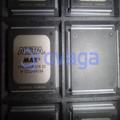
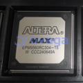
Altera EP2C70F896C6N

With 896 pins and housed in a fine-pitch ball grid array (FBGA) package


ブランド: Altera
製造元部品 #: EP2C70F896C6N
データシート: EP2C70F896C6N データシート (PDF)
パッケージ/ケース: FBGA-896
RoHS ステータス:
在庫状況: 2,399 個、新しいオリジナル
製品の種類: FPGAs (Field Programmable Gate Array)
Warranty: 1 Year Ovaga Warranty - Find Out More
0
1
*すべての価格は米ドルです
| 数量 | 単価 | 外部価格 |
|---|---|---|
| 1 | $2090.893 | $2090.893 |
| 189 | $834.280 | $157678.920 |
| 513 | $806.402 | $413684.226 |
| 999 | $792.626 | $791833.374 |
在庫あり: 2,399 PCS
EP2C70F896C6N 概要
The EP2C70F896C6N FPGA, a cornerstone of Altera's legacy now seamlessly integrated into Intel's portfolio, is a testament to relentless innovation in the realm of programmable logic devices. Boasting a formidable arsenal of 70,000 logic elements and 896 pins, it stands as a pinnacle of engineering prowess, designed to excel in mission-critical applications demanding both speed and efficiency. With its finely tuned architecture and comprehensive feature set—including embedded memory, DSP slices, and PLLs—it delivers unparalleled performance across diverse domains. Whether deployed in telecommunications infrastructure or automotive control systems, its adaptability and reconfigurability empower developers to push the boundaries of what's possible, ushering in a new era of computational agility and efficiency

仕様
| パラメータ | 価値 | パラメータ | 価値 |
|---|---|---|---|
| feature-family-name | Cyclone® II | feature-process-technology | 90nm |
| feature-maximum-number-of-user-i-os | 622 | feature-number-of-registers | |
| feature-device-logic-cells | 68416 | feature-device-system-gates | |
| feature-number-of-multipliers | 150 (18x18) | feature-program-memory-type | SRAM |
| feature-ram-bits-kbit | 1125 | feature-total-number-of-block-ram | 250 |
| feature-ethernet-macs | feature-supported-ip-core | 32/64-bit PCI-X bus Master/Target interface Core, 66/100/133Mhz|10 Gigabit Ethernet MAC|SpeedView Enabled JPEG Encoder (SVE-JPEG-E)|V1 ColdFire|Viterbi Compiler, Low-Speed/Hybrid Serial Decoder | |
| feature-supported-ip-core-manufacture | Altera/Freescale/CAST, Inc/MorethanIP/PLDA | feature-maximum-number-of-serdes-channels | |
| feature-device-logic-units | 68416 | feature-device-number-of-dlls-plls | 4 |
| feature-transceiver-blocks | feature-transceiver-speed-gbps | ||
| feature-dedicated-dsp | feature-pci-blocks | ||
| feature-programmability | No | feature-maximum-internal-frequency-mhz | 500 |
| feature-speed-grade | 6 | feature-giga-multiply-accumulates-per-second | |
| feature-differential-i-o-standards-supported | PCI-X|LVDS | feature-single-ended-i-o-standards-supported | PCI-X|LVDS |
| feature-external-memory-interface | QDR II+SRAM|DDR SDRAM | feature-minimum-operating-supply-voltage-v | 1.15 |
| feature-maximum-operating-supply-voltage-v | 1.25 | feature-packaging | |
| feature-rohs | feature-rad-hard | ||
| feature-pin-count | 896 | feature-supplier-package | FBGA |
| feature-standard-package-name1 | BGA | feature-cecc-qualified | No |
| feature-esd-protection | feature-escc-qualified | ||
| feature-military | No | feature-aec-qualified | No |
| feature-aec-qualified-number | feature-auto-motive | No | |
| feature-p-pap | No | feature-eccn-code | 3A991 |
| feature-svhc | No |
配送
| 配送タイプ | 配送料 | リードタイム | |
|---|---|---|---|
 |
DHL | $20.00-$40.00 (0.50 KG) | 2-5 日々 |
 |
フェデックス | $20.00-$40.00 (0.50 KG) | 2-5 日々 |
 |
UPS | $20.00-$40.00 (0.50 KG) | 2-5 日々 |
 |
TNT | $20.00-$40.00 (0.50 KG) | 2-5 日々 |
 |
EMS | $20.00-$40.00 (0.50 KG) | 2-5 日々 |
 |
登録された航空便 | $20.00-$40.00 (0.50 KG) | 2-5 日々 |
処理時間:送料は地域や国によって異なります。
支払い
| 支払条件 | ハンドフィー | |
|---|---|---|
 |
電信送金 | 銀行手数料 US$30.00 を請求します。 |
 |
ペイパル | 4.0%のサービス料がかかります。 |
 |
クレジットカード | 3.5%のサービス料がかかります。 |
 |
ウエスタンユニオン | charge US.00 banking fee. |
 |
送金サービス | 銀行手数料は 0.00 米ドルかかります。 |
保証
1.購入した電子部品には365日保証が含まれており、製品の品質を保証します。
2.受け取った商品の一部が完璧な品質ではない場合、当社は責任を持って返金または交換を手配します。 ただし、商品は元の状態のままでなければなりません。
パッキング
-

ステップ1 :製品
-

ステップ2 :真空包装
-

ステップ3 :静電気防止袋
-

ステップ4 :個包装
-

ステップ5 :梱包箱
-

ステップ6 :バーコード配送タグ


すべての製品は静電気防止袋に梱包されます。 ESD 帯電防止保護を備えた状態で出荷されます。
社外の ESD 梱包ラベルには、部品番号、ブランド、数量などの当社の情報が使用されます。
私たちは出荷前にすべての商品を検査し、すべての製品が良好な状態であることを確認し、部品が新しいオリジナルでデータシートと一致していることを確認します。
すべての商品に問題がないことを確認した後、梱包後、安全に梱包し、グローバルエクスプレスで発送します。 優れた耐穿刺性と耐引裂性を示し、シールの完全性も良好です。


パーツポイント
-
The EP2C70F896C6N is a field-programmable gate array (FPGA) chip from Altera. It features 70,000 logic elements, over 2.1 million bits of RAM, and 343 user I/Os. The chip offers versatile programmability for a wide range of applications, such as telecommunications, automotive, and industrial automation.
-
Equivalent
Some equivalent products of the EP2C70F896C6N chip are Altera Cyclone II EP2C70F896C6, Intel Cyclone II EP2C70F896C6, and other FPGAs from the same family with similar specifications and features. These chips are commonly used for low-cost, entry-level FPGA development and prototyping. -
Features
EP2C70F896C6N is an FPGA device from Altera's Cyclone II family. It features 70,000 logic elements (LEs), 376 embedded memory blocks, 196 embedded 18 x 18 multipliers, and a maximum of 896 user I/Os. It operates on a 1.5V core voltage and supports various I/O standards. -
Pinout
The EP2C70F896C6N is a Field-Programmable Gate Array (FPGA) from Intel (formerly Altera) with a pin count of 896. It features 70,000 logic elements, 2060 kbits of embedded memory, and 220 DSP blocks. The device is used for implementing complex digital designs in various applications such as telecommunications, industrial automation, and signal processing. -
Manufacturer
The EP2C70F896C6N is manufactured by Intel Corporation, a multinational technology company known for its computing and communications products. They specialize in the design and production of processors, integrated circuits, and other hardware components used in a variety of devices and systems worldwide. -
Application Field
The EP2C70F896C6N is a field-programmable gate array (FPGA) commonly used in various applications such as industrial automation, automotive electronics, telecommunications, and aerospace. Its high processing power, programmability, and parallel processing capabilities make it ideal for applications requiring high performance, low latency, and reliability. -
Package
The EP2C70F896C6N chip is a Field Programmable Gate Array (FPGA) in an FBGA (Fine Pitch Ball Grid Array) package. It is in the form of a silicon chip, and the size is 27 x 27 mm with a 896-ball grid array (27 x 27, 0.8mm pitch).


私たちは高品質の製品、思いやりのあるサービス、販売後の保証を提供します
-

豊富な商品を取り揃えておりますので、お客様の様々なニーズにお応え致します。
-

最小注文数量は1個からとなります。
-

最低国際配送料は0.00ドルから
-

全商品365日品質保証


