


画像は参考用です。製品仕様を参照してください。
注文金額が
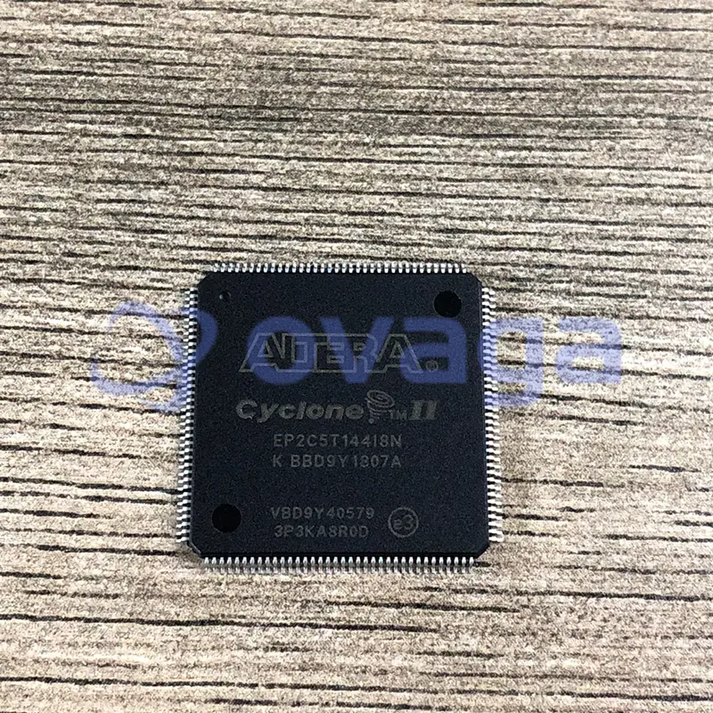
$5000Altera EP2C5T144I8N
Voltage Requirement of 1.2V


ブランド: Altera Corporation (Intel)
製造元部品 #: EP2C5T144I8N
データシート: EP2C5T144I8N Datasheet (PDF)
パッケージ/ケース: TQFP-144
EP2C5T144I8N 概要
With its compact form factor and robust feature set, the EP2C5T144I8N FPGA is a versatile tool for engineers and developers seeking to push the boundaries of technology. Its blend of advanced capabilities, including high-speed operation and ample memory resources, makes it a suitable choice for a wide range of applications. From prototyping new consumer electronics devices to optimizing communication systems, this FPGA offers the flexibility and performance required to bring innovative ideas to life. In an increasingly digital world, having access to cutting-edge hardware like the EP2C5T144I8N can make all the difference in turning concepts into reality
特徴
- The EP2C5T144I8N FPGA has 5,120 logic elements (LEs) and 18,752 adaptive logic modules (ALMs).
- It has a maximum of 36 embedded multipliers and 288 18x18-bit embedded memory blocks.
- The device operates at a maximum frequency of 250 MHz and has a total of 120 I/O pins.
- The FPGA is programmed using the Quartus II development software and supports a range of interfaces such as JTAG, SPI, and I2C.
応用
- Digital signal processing
- Video and image processing
- Control systems
- Communication systems
- Industrial automation
仕様
| パラメータ | 価値 | パラメータ | 価値 |
|---|---|---|---|
| feature-family-name | Cyclone® II | feature-process-technology | 90nm |
| feature-maximum-number-of-user-i-os | 89 | feature-number-of-registers | |
| feature-device-logic-cells | 4608 | feature-device-system-gates | |
| feature-number-of-multipliers | 13 (18x18) | feature-program-memory-type | SRAM |
| feature-ram-bits-kbit | 117 | feature-total-number-of-block-ram | 26 |
| feature-ethernet-macs | feature-supported-ip-core | Viterbi Compiler, Low-Speed/Hybrid Serial Decoder|V1 ColdFire|SpeedView Enabled JPEG Encoder (SVE-JPEG-E)|10 Gigabit Ethernet MAC|32/64-bit PCI-X bus Master/Target interface Core, 66/100/133Mhz | |
| feature-supported-ip-core-manufacture | Altera/Freescale/CAST, Inc/MorethanIP/PLDA | feature-maximum-number-of-serdes-channels | |
| feature-device-logic-units | 4608 | feature-device-number-of-dlls-plls | 2 |
| feature-transceiver-blocks | feature-transceiver-speed-gbps | ||
| feature-dedicated-dsp | feature-pci-blocks | ||
| feature-programmability | No | feature-maximum-internal-frequency-mhz | 402.58 |
| feature-speed-grade | 8 | feature-giga-multiply-accumulates-per-second | |
| feature-differential-i-o-standards-supported | LVDS|PCI-X | feature-single-ended-i-o-standards-supported | LVDS|PCI-X |
| feature-external-memory-interface | DDR SDRAM|QDR II+SRAM | feature-minimum-operating-supply-voltage-v | 1.15 |
| feature-maximum-operating-supply-voltage-v | 1.25 | feature-packaging | |
| feature-rohs | feature-rad-hard | ||
| feature-pin-count | 144 | feature-supplier-package | TQFP |
| feature-standard-package-name1 | QFP | feature-cecc-qualified | No |
| feature-esd-protection | feature-escc-qualified | ||
| feature-military | No | feature-aec-qualified | No |
| feature-aec-qualified-number | feature-auto-motive | No | |
| feature-p-pap | No | feature-eccn-code | EAR99 |
| feature-svhc | No |
配送
| 配送タイプ | 配送料 | リードタイム | |
|---|---|---|---|
 |
DHL | $20.00-$40.00 (0.50 KG) | 2-5 日々 |
 |
フェデックス | $20.00-$40.00 (0.50 KG) | 2-5 日々 |
 |
UPS | $20.00-$40.00 (0.50 KG) | 2-5 日々 |
 |
TNT | $20.00-$40.00 (0.50 KG) | 2-5 日々 |
 |
EMS | $20.00-$40.00 (0.50 KG) | 2-5 日々 |
 |
登録された航空便 | $20.00-$40.00 (0.50 KG) | 2-5 日々 |
処理時間:送料は地域や国によって異なります。
支払い
| 支払条件 | ハンドフィー | |
|---|---|---|
 |
電信送金 | 銀行手数料 US$30.00 を請求します。 |
 |
ペイパル | 4.0%のサービス料がかかります。 |
 |
クレジットカード | 3.5%のサービス料がかかります。 |
 |
ウエスタンユニオン | charge US.00 banking fee. |
 |
送金サービス | 銀行手数料は 0.00 米ドルかかります。 |
保証
1.購入した電子部品には365日保証が含まれており、製品の品質を保証します。
2.受け取った商品の一部が完璧な品質ではない場合、当社は責任を持って返金または交換を手配します。 ただし、商品は元の状態のままでなければなりません。
パッキング
-

ステップ1 :製品
-

ステップ2 :真空包装
-

ステップ3 :静電気防止袋
-

ステップ4 :個包装
-

ステップ5 :梱包箱
-

ステップ6 :バーコード配送タグ


すべての製品は静電気防止袋に梱包されます。 ESD 帯電防止保護を備えた状態で出荷されます。
社外の ESD 梱包ラベルには、部品番号、ブランド、数量などの当社の情報が使用されます。
私たちは出荷前にすべての商品を検査し、すべての製品が良好な状態であることを確認し、部品が新しいオリジナルでデータシートと一致していることを確認します。
すべての商品に問題がないことを確認した後、梱包後、安全に梱包し、グローバルエクスプレスで発送します。 優れた耐穿刺性と耐引裂性を示し、シールの完全性も良好です。


同等部品
のために EP2C5T144I8N コンポーネントの場合は、これらの交換部品および代替部品を検討してください:
部品番号
ブランド
パッケージ
説明
部品番号 : EP2C5F256C8N
ブランド :
パッケージ : FBGA-256
説明 : FPGA Cyclone® II Family 4608 Cells 402.58MHz 90nm Technology 1.2V
部品番号 : EP2C5T144C8N
ブランド :
パッケージ : TQFP-144
説明 : FPGA - Field Programmable Gate Array FPGA - Cyclone II 288 LABs 89 IOs
部品番号 : EP2C5T144C6N
ブランド :
パッケージ : TQFP-144
説明 : FPGA Cyclone® II Family 4608 Cells 500MHz 90nm Technology 1.2V 144-Pin TQFP
部品番号 : EP2C5T144I6N
ブランド :
パッケージ :
説明 :
部品番号 : EP2C5T144C7N
ブランド :
パッケージ : TQFP-144
説明 : FPGA Cyclone® II Family 4608 Cells 402.58MHz 90nm Technology 1.2V
パーツポイント
-
The EP2C5T144I8N chip is a field-programmable gate array (FPGA) produced by Altera (now Intel). It belongs to the Cyclone II family and offers 5,008 logic elements, 72 embedded memory blocks, and 7 phase-locked loops. The chip allows users to configure its logic functions after manufacturing, making it highly versatile for various applications such as digital signal processing and embedded systems.
-
Equivalent
Some equivalent products to the EP2C5T144I8N chip include the EP2C5T144C8N, EP2C5T144C7N, and EP2C5Q208C8N. These chips have similar functionality and specifications but may vary in certain features or packaging options. -
Features
The EP2C5T144I8N is a Cyclone II FPGA, with 5,136 logic elements, 266 user I/Os, and 4 PLLs. It operates at a maximum frequency of 300 MHz and has 132,304 bits of embedded memory. It has various configuration options and supports 1.2V and 2.5V power supplies. -
Manufacturer
The manufacturer of the EP2C5T144I8N is Altera (now owned by Intel). It is a semiconductor company that specializes in developing programmable logic devices, systems-on-chips (SoCs), and other related products. -
Application Field
The EP2C5T144I8N is an FPGA (Field-Programmable Gate Array) chip commonly used for prototyping and development in various applications. It finds application in industries such as telecommunications, aerospace, automotive, and consumer electronics. It is used to implement and test complex digital designs, perform signal processing, accelerate computational tasks, and enable hardware acceleration in different devices and systems. -
Package
The EP2C5T144I8N chip has a package type of TQFP (Thin Quad Flat Pack), a form of surface mount technology. It has a size of 14mm x 14mm, with a total of 144 pins in a grid pattern.


データシート PDF
私たちは高品質の製品、思いやりのあるサービス、販売後の保証を提供します
-

豊富な商品を取り揃えておりますので、お客様の様々なニーズにお応え致します。
-

最小注文数量は1個からとなります。
-

最低国際配送料は0.00ドルから
-

全商品365日品質保証


