

画像は参考用です。製品仕様を参照してください。
注文金額が
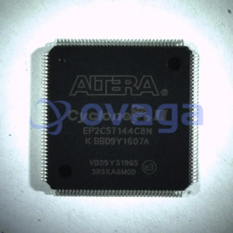
$5000Altera EP2C5T144C8
The FPGA EP2C5T144C8 features a Field Programmable Gate Array architecture


ブランド: Altera Corporation (Intel)
製造元部品 #: EP2C5T144C8
データシート: EP2C5T144C8 データシート (PDF)
パッケージ/ケース: TQFP-144
EP2C5T144C8 概要
The EP2C5T144C8 from Altera is a Cyclone II FPGA with 5,136 logic elements and 140 Logic Array Blocks (LABs), offering 2,736 Kbits of embedded memory and 144 pins, including 82 user I/O pins. Operating at a maximum clock frequency of 250 MHz, this FPGA provides fast processing speeds for real-time applications and includes dedicated PLLs for clock management and synchronization. With support for communication interfaces such as SPI, UART, and I2C, it is suitable for interfacing with sensors, displays, and other external devices. Additionally, the EP2C5T144C8 is highly configurable and can be programmed using the Quartus II software tool, allowing users to implement custom logic functions, optimize performance, and meet specific design requirements. Housed in a compact 144-pin TQFP package, this FPGA is well-suited for small form factor designs, making it an ideal choice for a wide range of electronic applications
 Inventory")
仕様
| パラメータ | 価値 | パラメータ | 価値 |
|---|---|---|---|
| feature-family-name | Cyclone® II | feature-process-technology | 90nm |
| feature-maximum-number-of-user-i-os | 89 | feature-number-of-registers | |
| feature-device-logic-cells | 4608 | feature-device-system-gates | |
| feature-number-of-multipliers | 13 (18x18) | feature-program-memory-type | SRAM |
| feature-ram-bits-kbit | 117 | feature-total-number-of-block-ram | 26 |
| feature-ethernet-macs | feature-supported-ip-core | Viterbi Compiler, Low-Speed/Hybrid Serial Decoder|V1 ColdFire|SpeedView Enabled JPEG Encoder (SVE-JPEG-E)|10 Gigabit Ethernet MAC|32/64-bit PCI-X bus Master/Target interface Core, 66/100/133Mhz | |
| feature-supported-ip-core-manufacture | Altera/Freescale/CAST, Inc/MorethanIP/PLDA | feature-maximum-number-of-serdes-channels | |
| feature-device-logic-units | 4608 | feature-device-number-of-dlls-plls | 2 |
| feature-transceiver-blocks | feature-transceiver-speed-gbps | ||
| feature-dedicated-dsp | feature-pci-blocks | ||
| feature-programmability | No | feature-maximum-internal-frequency-mhz | 402.58 |
| feature-speed-grade | 8 | feature-giga-multiply-accumulates-per-second | |
| feature-differential-i-o-standards-supported | LVDS|PCI-X | feature-single-ended-i-o-standards-supported | LVDS|PCI-X |
| feature-external-memory-interface | DDR SDRAM|QDR II+SRAM | feature-minimum-operating-supply-voltage-v | 1.15 |
| feature-maximum-operating-supply-voltage-v | 1.25 | feature-packaging | |
| feature-rohs | feature-rad-hard | ||
| feature-pin-count | 144 | feature-supplier-package | TQFP |
| feature-standard-package-name1 | QFP | feature-cecc-qualified | No |
| feature-esd-protection | feature-escc-qualified | ||
| feature-military | No | feature-aec-qualified | No |
| feature-aec-qualified-number | feature-auto-motive | No | |
| feature-p-pap | No | feature-eccn-code | EAR99 |
| feature-svhc |
配送
| 配送タイプ | 配送料 | リードタイム | |
|---|---|---|---|
 |
DHL | $20.00-$40.00 (0.50 KG) | 2-5 日々 |
 |
フェデックス | $20.00-$40.00 (0.50 KG) | 2-5 日々 |
 |
UPS | $20.00-$40.00 (0.50 KG) | 2-5 日々 |
 |
TNT | $20.00-$40.00 (0.50 KG) | 2-5 日々 |
 |
EMS | $20.00-$40.00 (0.50 KG) | 2-5 日々 |
 |
登録された航空便 | $20.00-$40.00 (0.50 KG) | 2-5 日々 |
処理時間:送料は地域や国によって異なります。
支払い
| 支払条件 | ハンドフィー | |
|---|---|---|
 |
電信送金 | 銀行手数料 US$30.00 を請求します。 |
 |
ペイパル | 4.0%のサービス料がかかります。 |
 |
クレジットカード | 3.5%のサービス料がかかります。 |
 |
ウエスタンユニオン | charge US.00 banking fee. |
 |
送金サービス | 銀行手数料は 0.00 米ドルかかります。 |
保証
1.購入した電子部品には365日保証が含まれており、製品の品質を保証します。
2.受け取った商品の一部が完璧な品質ではない場合、当社は責任を持って返金または交換を手配します。 ただし、商品は元の状態のままでなければなりません。
パッキング
-

ステップ1 :製品
-

ステップ2 :真空包装
-

ステップ3 :静電気防止袋
-

ステップ4 :個包装
-

ステップ5 :梱包箱
-

ステップ6 :バーコード配送タグ


すべての製品は静電気防止袋に梱包されます。 ESD 帯電防止保護を備えた状態で出荷されます。
社外の ESD 梱包ラベルには、部品番号、ブランド、数量などの当社の情報が使用されます。
私たちは出荷前にすべての商品を検査し、すべての製品が良好な状態であることを確認し、部品が新しいオリジナルでデータシートと一致していることを確認します。
すべての商品に問題がないことを確認した後、梱包後、安全に梱包し、グローバルエクスプレスで発送します。 優れた耐穿刺性と耐引裂性を示し、シールの完全性も良好です。


パーツポイント
-
EP2C5T144C8 is a programmable logic chip by Intel's Altera. It belongs to the Cyclone II FPGA family and comes in a 144-pin TQFP package. It offers 4,608 logic elements, 75,000 gates, and 368 RAM blocks. With a speed grade of C8, it operates at a maximum frequency of 240 MHz. This chip provides flexibility for implementing various digital circuits and is commonly used in applications requiring high-performance and low-cost FPGA solutions.
-
Features
The EP2C5T144C8 is an Altera Cyclone II FPGA with 5,120 logic elements, 4 PLLs, and 50 I/O pins. It operates at a maximum frequency of 260 MHz and has 144-pin TQFP packaging. It is a low-power and cost-effective solution for small-scale digital designs and applications. -
Pinout
The EP2C5T144C8 is a Field Programmable Gate Array (FPGA) with a pin count of 144. It is used to implement digital circuits and offers reconfigurable logic elements. The specific functions of each pin would depend on the design and programming of the FPGA. -
Manufacturer
ALTERA is the manufacturer of the EP2C5T144C8. It is a semiconductor company specializing in programmable logic devices and related software. -
Application Field
The EP2C5T144C8 is a Field-Programmable Gate Array (FPGA) that is commonly used in various application areas, including telecommunications, medical devices, automotive electronics, industrial automation, and consumer electronics. Its versatility, programmability, and ability to handle complex tasks make it suitable for a wide range of applications. -
Package
The EP2C5T144C8 chip has a package type of 144-TQFP and a size of 20mm x 20mm.


私たちは高品質の製品、思いやりのあるサービス、販売後の保証を提供します
-

豊富な商品を取り揃えておりますので、お客様の様々なニーズにお応え致します。
-

最小注文数量は1個からとなります。
-

最低国際配送料は0.00ドルから
-

全商品365日品質保証


