

画像は参考用です。製品仕様を参照してください。
注文金額が
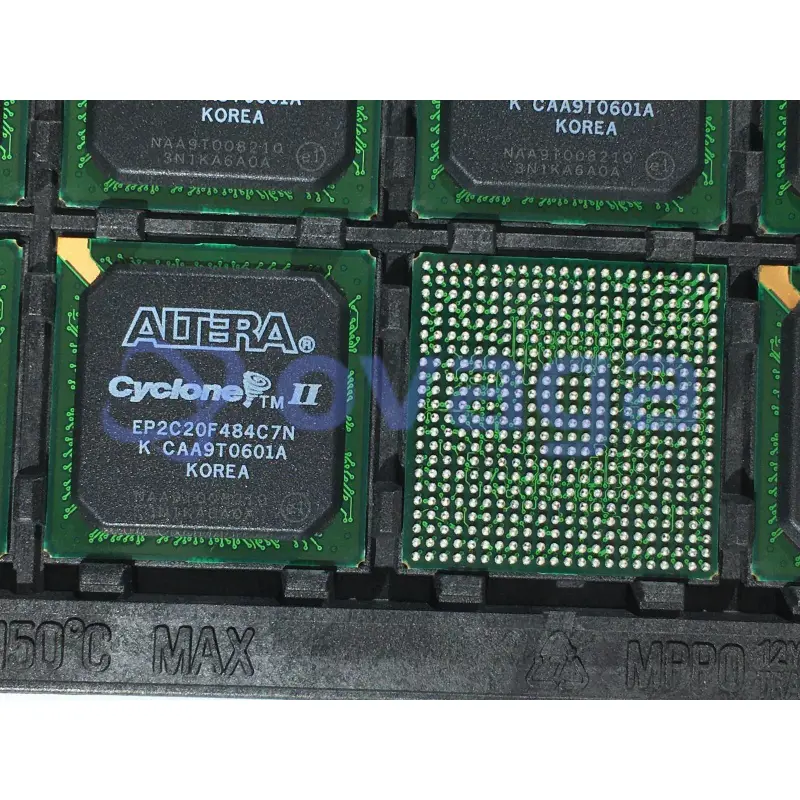
$5000Altera EP2C20F484C7N
Maximum frequency of 402.58MHz


ブランド: Altera Corporation (Intel)
製造元部品 #: EP2C20F484C7N
データシート: EP2C20F484C7N データシート (PDF)
パッケージ/ケース: FBGA-484
EP2C20F484C7N 概要
The EP2C20F484C7N FPGA device by Intel, part of the Cyclone II series, offers a powerful combination of features for versatile hardware design applications. With a generous amount of Logic Elements (LEs) totaling 19808 and 414 Embedded Multiplier 9-bit blocks, designers have ample resources to implement complex logic and arithmetic functions. The device also includes 114 embedded 18 x 18 multipliers, 576 Kbits of embedded memory, and up to 480 user I/O pins, providing flexibility for a wide range of connectivity options
 Inventory")
仕様
| パラメータ | 価値 | パラメータ | 価値 |
|---|---|---|---|
| feature-family-name | Cyclone® II | feature-process-technology | 90nm |
| feature-maximum-number-of-user-i-os | 315 | feature-number-of-registers | |
| feature-device-logic-cells | 18752 | feature-device-system-gates | |
| feature-number-of-multipliers | 26 (18x18) | feature-program-memory-type | SRAM |
| feature-ram-bits-kbit | 234 | feature-total-number-of-block-ram | 52 |
| feature-ethernet-macs | feature-supported-ip-core | Viterbi Compiler, Low-Speed/Hybrid Serial Decoder|V1 ColdFire|SpeedView Enabled JPEG Encoder (SVE-JPEG-E)|10 Gigabit Ethernet MAC|32/64-bit PCI-X bus Master/Target interface Core, 66/100/133Mhz | |
| feature-supported-ip-core-manufacture | Altera/Freescale/CAST, Inc/MorethanIP/PLDA | feature-maximum-number-of-serdes-channels | |
| feature-device-logic-units | 18752 | feature-device-number-of-dlls-plls | 4 |
| feature-transceiver-blocks | feature-transceiver-speed-gbps | ||
| feature-dedicated-dsp | feature-pci-blocks | ||
| feature-programmability | No | feature-maximum-internal-frequency-mhz | 402.58 |
| feature-speed-grade | 7 | feature-giga-multiply-accumulates-per-second | |
| feature-differential-i-o-standards-supported | LVDS|PCI-X | feature-single-ended-i-o-standards-supported | LVDS|PCI-X |
| feature-external-memory-interface | DDR SDRAM|QDR II+SRAM | feature-minimum-operating-supply-voltage-v | 1.15 |
| feature-maximum-operating-supply-voltage-v | 1.25 | feature-packaging | Tray |
| feature-rohs | feature-rad-hard | ||
| feature-pin-count | 484 | feature-supplier-package | FBGA |
| feature-standard-package-name1 | BGA | feature-cecc-qualified | No |
| feature-esd-protection | feature-escc-qualified | ||
| feature-military | No | feature-aec-qualified | No |
| feature-aec-qualified-number | feature-auto-motive | No | |
| feature-p-pap | No | feature-eccn-code | 3A991 |
| feature-svhc | Yes |
配送
| 配送タイプ | 配送料 | リードタイム | |
|---|---|---|---|
 |
DHL | $20.00-$40.00 (0.50 KG) | 2-5 日々 |
 |
フェデックス | $20.00-$40.00 (0.50 KG) | 2-5 日々 |
 |
UPS | $20.00-$40.00 (0.50 KG) | 2-5 日々 |
 |
TNT | $20.00-$40.00 (0.50 KG) | 2-5 日々 |
 |
EMS | $20.00-$40.00 (0.50 KG) | 2-5 日々 |
 |
登録された航空便 | $20.00-$40.00 (0.50 KG) | 2-5 日々 |
処理時間:送料は地域や国によって異なります。
支払い
| 支払条件 | ハンドフィー | |
|---|---|---|
 |
電信送金 | 銀行手数料 US$30.00 を請求します。 |
 |
ペイパル | 4.0%のサービス料がかかります。 |
 |
クレジットカード | 3.5%のサービス料がかかります。 |
 |
ウエスタンユニオン | charge US.00 banking fee. |
 |
送金サービス | 銀行手数料は 0.00 米ドルかかります。 |
保証
1.購入した電子部品には365日保証が含まれており、製品の品質を保証します。
2.受け取った商品の一部が完璧な品質ではない場合、当社は責任を持って返金または交換を手配します。 ただし、商品は元の状態のままでなければなりません。
パッキング
-

ステップ1 :製品
-

ステップ2 :真空包装
-

ステップ3 :静電気防止袋
-

ステップ4 :個包装
-

ステップ5 :梱包箱
-

ステップ6 :バーコード配送タグ


すべての製品は静電気防止袋に梱包されます。 ESD 帯電防止保護を備えた状態で出荷されます。
社外の ESD 梱包ラベルには、部品番号、ブランド、数量などの当社の情報が使用されます。
私たちは出荷前にすべての商品を検査し、すべての製品が良好な状態であることを確認し、部品が新しいオリジナルでデータシートと一致していることを確認します。
すべての商品に問題がないことを確認した後、梱包後、安全に梱包し、グローバルエクスプレスで発送します。 優れた耐穿刺性と耐引裂性を示し、シールの完全性も良好です。


パーツポイント
-
The Altera EP2C20F484C7N is a Field-Programmable Gate Array (FPGA) chip with 20,000 logic elements, 484 pins, and 7ns maximum delay. It offers flexibility for implementing custom digital circuits and is often used in telecommunications, automotive, and industrial applications.
-
Equivalent
Some equivalent products of EP2C20F484C7N chip include Altera EP2C20F484C8N, Altera EP2C20F484I7N, Altera EP2C20F484I8N, and Altera EP2C20F484I7N. These chips are part of the Cyclone II FPGA family and offer similar features and functionalities to the EP2C20F484C7N chip. -
Features
The EP2C20F484C7N is a FPGA that features 19,008 logic elements, 356KB embedded memory, 504 18x18 multipliers, and 2.5V core voltage. It also has 292 I/O pins, 2 DLLs, and supports configuration through JTAG. This FPGA is ideal for applications such as signal processing, video processing, and image processing. -
Pinout
The EP2C20F484C7N is a Cyclone II FPGA with 484 pins. It is a field-programmable gate array used for digital logic applications such as signal processing, data processing, and communication. The pins on the device can be configured to serve different functions based on the design requirements. -
Manufacturer
The EP2C20F484C7N is manufactured by Intel Corporation. Intel Corporation is an American multinational corporation that designs and manufactures semiconductor products and related software. It is one of the world's largest and highest valued semiconductor chip makers based on revenue. -
Application Field
Some application areas of the EP2C20F484C7N include industrial automation, communications, automotive, and consumer electronics. It is typically used for designing embedded systems, digital signal processing, and control systems. Its advanced features, such as programmable logic, high-speed serial transceivers, and memory resources, make it suitable for a wide range of applications. -
Package
The EP2C20F484C7N chip is in a ball grid array (BGA) package type, with a form factor of 484 balls. It measures 17mm x 17mm in size.


私たちは高品質の製品、思いやりのあるサービス、販売後の保証を提供します
-

豊富な商品を取り揃えておりますので、お客様の様々なニーズにお応え致します。
-

最小注文数量は1個からとなります。
-

最低国際配送料は0.00ドルから
-

全商品365日品質保証


