

画像は参考用です。製品仕様を参照してください。
注文金額が
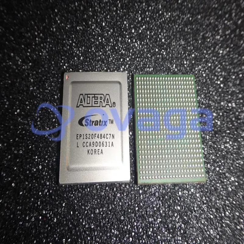
$5000Intel EP1S20F484C7N
The EP1S20F484C7N is a high-performance FPGA from the Stratix® family, featuring 18460 cells and operating at a frequency of 420.17MHz


EP1S20F484C7N 概要
The EP1S20F484C7N FPGA is a versatile component from the Altera Stratix II series, offering a balanced combination of logic elements, package type, speed grade, and temperature range. With 20 thousand logic elements, it provides a moderate amount of computational power suitable for a wide range of applications. The F484 package type ensures compatibility with 484-pin FineLine BGA sockets, making it easy to integrate into existing electronic systems. The C7 speed grade indicates optimal performance levels, catering to demanding computational tasks. Additionally, the N temperature range allows for reliable operation in commercial environments with temperatures ranging from 0°C to 85°C. For detailed technical specifications and features, referencing the datasheet is essential to fully understand the capabilities and limitations of this FPGA
特徴
Configuration devices for SRAM-based LUT devices offer the following features:
Configures Altera ACEX 1K, APEX 20K (including APEX 20K, APEX 20KC, and APEX 20KE), APEX II, Arria GX, Cyclone, Cyclone II, FLEX 10K (including FLEX 10KE and FLEX 10KA) Mercury, Stratix, Stratix GX, Stratix II, and Stratix II GX devices
Easy-to-use four-pin interface
Low current during configuration and near-zero standby mode current
Programming support with the Altera Programming Unit (APU) and programming hardware from Data I/O, BP Microsystems, and other third-party programmers
Available in compact plastic packages
8-pin plastic dual in-line (PDIP) package
20-pin plastic J-lead chip carrier (PLCC) package
32-pin plastic thin quad flat pack (TQFP) package
EPC2 device has reprogrammable flash configuration memory
5.0-V and 3.3-V in-system programmability (ISP) through the built-in IEEE Std.
1149.1 JTAG interface
Built-in JTAG boundary-scan test (BST) circuitry compliant with IEEE Std. 1149.1
Supports programming through Serial Vector Format File (.svf), Jam Standard Test and Programming Language (STAPL) Format File (.jam), JAM Byte Code File (.jbc), and the Quartus II and MAX+PLUS II softwares using the USB-Blaster, MasterBlaster, ByteBlaster II, EthernetBlaster, or ByteBlasterMV download cable
Supports programming through Programmer Object File (.pof) for EPC1 and EPC1441 devices
nINIT_CONF pin allows INIT_CONF JTAG instruction to begin FPGA configuration

仕様
| パラメータ | 価値 | パラメータ | 価値 |
|---|---|---|---|
| Manufacturer: | Intel | Product Category: | FPGA - Field Programmable Gate Array |
| Shipping Restrictions: | This product may require additional documentation to export from the United States. | RoHS: | Details |
| Series: | Stratix EP1S20 | Number of Logic Elements: | 18460 LE |
| Adaptive Logic Modules - ALMs: | - | Embedded Memory: | 1.59 Mbit |
| Number of I/Os: | 361 I/O | Supply Voltage - Min: | 1.5 V |
| Supply Voltage - Max: | 1.5 V | Minimum Operating Temperature: | 0 C |
| Maximum Operating Temperature: | + 70 C | Mounting Style: | SMD/SMT |
| Package / Case: | FBGA-484 | Packaging: | Tray |
| Brand: | Intel / Altera | Maximum Operating Frequency: | 66 MHz |
| Moisture Sensitive: | Yes | Number of Logic Array Blocks - LABs: | 1846 LAB |
| Operating Supply Current: | 65 mA | Operating Supply Voltage: | 1.5 V |
| Product Type: | FPGA - Field Programmable Gate Array | Factory Pack Quantity: | 60 |
| Subcategory: | Programmable Logic ICs | Total Memory: | 1669248 bit |
| Tradename: | Stratix |
配送
| 配送タイプ | 配送料 | リードタイム | |
|---|---|---|---|
 |
DHL | $20.00-$40.00 (0.50 KG) | 2-5 日々 |
 |
フェデックス | $20.00-$40.00 (0.50 KG) | 2-5 日々 |
 |
UPS | $20.00-$40.00 (0.50 KG) | 2-5 日々 |
 |
TNT | $20.00-$40.00 (0.50 KG) | 2-5 日々 |
 |
EMS | $20.00-$40.00 (0.50 KG) | 2-5 日々 |
 |
登録された航空便 | $20.00-$40.00 (0.50 KG) | 2-5 日々 |
処理時間:送料は地域や国によって異なります。
支払い
| 支払条件 | ハンドフィー | |
|---|---|---|
 |
電信送金 | 銀行手数料 US$30.00 を請求します。 |
 |
ペイパル | 4.0%のサービス料がかかります。 |
 |
クレジットカード | 3.5%のサービス料がかかります。 |
 |
ウエスタンユニオン | charge US.00 banking fee. |
 |
送金サービス | 銀行手数料は 0.00 米ドルかかります。 |
保証
1.購入した電子部品には365日保証が含まれており、製品の品質を保証します。
2.受け取った商品の一部が完璧な品質ではない場合、当社は責任を持って返金または交換を手配します。 ただし、商品は元の状態のままでなければなりません。
パッキング
-

ステップ1 :製品
-

ステップ2 :真空包装
-

ステップ3 :静電気防止袋
-

ステップ4 :個包装
-

ステップ5 :梱包箱
-

ステップ6 :バーコード配送タグ


すべての製品は静電気防止袋に梱包されます。 ESD 帯電防止保護を備えた状態で出荷されます。
社外の ESD 梱包ラベルには、部品番号、ブランド、数量などの当社の情報が使用されます。
私たちは出荷前にすべての商品を検査し、すべての製品が良好な状態であることを確認し、部品が新しいオリジナルでデータシートと一致していることを確認します。
すべての商品に問題がないことを確認した後、梱包後、安全に梱包し、グローバルエクスプレスで発送します。 優れた耐穿刺性と耐引裂性を示し、シールの完全性も良好です。


パーツポイント
-
The EP1S20F484C7N chip is a field-programmable gate array (FPGA) manufactured by Altera (now part of Intel). It has 20,060 logic elements, 3,072 Kbits of embedded memory, and operates at a maximum frequency of 315 MHz. The chip also supports various I/O interfaces and can be configured to implement complex digital logic circuits.
-
Equivalent
Some equivalent products of the EP1S20F484C7N chip include the EP1S10F484C7, EP1S40F1020C7, and EP1S30F1020C7. These chips belong to the same family of Altera Stratix devices and have similar features and capabilities. -
Features
The EP1S20F484C7N is an Altera Stratix EP1S20 FPGA with 20,060 logic elements, 768 Kb RAM, 96 DSP blocks, and 16 PLLs. It operates at a maximum frequency of 330 MHz, has 484 pins, and supports configuration through JTAG interface. -
Pinout
The EP1S20F484C7N is a Field-Programmable Gate Array (FPGA) with 484 pins. The specific functions of each pin can vary depending on the specific design and configuration programmed onto the device. -
Manufacturer
The manufacturer of the EP1S20F484C7N is Intel Corporation. It is an American multinational technology company specializing in the design and manufacturing of integrated circuits and related products. -
Application Field
The EP1S20F484C7N is a programmable logic device (PLD) used in various applications. It can be commonly found in industrial automation, telecommunications, networking, and automotive control systems. With its high-performance capabilities and versatile features, this PLD can be utilized in a wide range of electronic systems requiring customizable logic functions. -
Package
The EP1S20F484C7N chip has a BGA (Ball Grid Array) package type, a 484-pin form, and a size of 1.097 inch x 1.097 inch, or approximately 27.86 mm x 27.86 mm.


私たちは高品質の製品、思いやりのあるサービス、販売後の保証を提供します
-

豊富な商品を取り揃えておりますので、お客様の様々なニーズにお応え致します。
-

最小注文数量は1個からとなります。
-

最低国際配送料は0.00ドルから
-

全商品365日品質保証


