


画像は参考用です。製品仕様を参照してください。
注文金額が
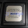
$5000Altera EP1C6F256C8N
Programmable Logic Device (CPLDs/FPGAs) EP1C6F256C8N in FBGA-256 package, ROHS Compliant


ブランド: Altera Corporation (Intel)
製造元部品 #: EP1C6F256C8N
データシート: EP1C6F256C8N Datasheet (PDF)
パッケージ/ケース: FBGA-256
EP1C6F256C8N 概要
The EP1C6F256C8N is a highly capable FPGA designed to meet the demands of modern electronic systems. With 598 logic blocks and 5980 macrocells, it provides substantial resources for implementing complex digital designs. The device features 256 pins and supports 8 speed grades, offering flexibility in interfacing with external components and achieving targeted performance levels. Operating with a core supply voltage range of 1.425V to 1.575V and an I/O supply voltage of 3.3V, it ensures efficient power utilization while meeting interface compatibility requirements. The integration of a PLL for clock management enables precise control over timing signals, contributing to overall system stability and reliability. Supporting various I/O interface standards including LVCMOS, LVDS, LVTTL, PCI, SSTL-2, and SSTL-3, this FPGA caters to a wide range of connectivity needs. With an operating temperature range of 0°C to +85°C, it is well-suited for deployment in diverse operating environments. Additionally, as a surface mount device, the EP1C6F256C8N offers ease of integration into PCB designs, streamlining the overall development process. In summary, this FPGA is a versatile and high-performance solution suitable for applications in industries such as telecommunications, automotive, and industrial control systems
特徴
- It has 6,144 logic elements (LEs) that can be programmed to perform specific logic functions.
- It has 256 embedded memory blocks (total memory of 810Kbits).
- It has 192 18x18-bit multipliers that can be used for digital signal processing (DSP) applications.
- It has four phase-locked loops (PLLs) that can generate clock signals with low jitter.
応用
- EP1C6F256C8N can be used in various applications such as communication, video and image processing, digital signal processing, control systems, and embedded systems.
- It can be used for implementing complex digital systems in hardware, providing faster performance compared to software implementation.
- It can also be used for prototyping and testing of ASIC designs.
仕様
| パラメータ | 価値 | パラメータ | 価値 |
|---|---|---|---|
| Product Name | EP1C6F256C8N | Product Type | FPGA |
| Manufacturer | Intel | Series | Cyclone |
| Number of Logic Elements | 5,910 | Number of LABs/CLBs | 1,472 |
| Number of IOs | 221 | Embedded Memory Size | 256,000 Bits |
| Embedded Memory Type | RAM | Operating Temperature | 0°C ~ 85°C |
| Voltage - Supply | 2.375 V ~ 2.625 V | Package / Case | 256-PBGA |
| Mounting Type | Surface Mount | Configuration | Non-Volatile |
| Number of RAM Bits | 256,000 |
配送
| 配送タイプ | 配送料 | リードタイム | |
|---|---|---|---|
 |
DHL | $20.00-$40.00 (0.50 KG) | 2-5 日々 |
 |
フェデックス | $20.00-$40.00 (0.50 KG) | 2-5 日々 |
 |
UPS | $20.00-$40.00 (0.50 KG) | 2-5 日々 |
 |
TNT | $20.00-$40.00 (0.50 KG) | 2-5 日々 |
 |
EMS | $20.00-$40.00 (0.50 KG) | 2-5 日々 |
 |
登録された航空便 | $20.00-$40.00 (0.50 KG) | 2-5 日々 |
処理時間:送料は地域や国によって異なります。
支払い
| 支払条件 | ハンドフィー | |
|---|---|---|
 |
電信送金 | 銀行手数料 US$30.00 を請求します。 |
 |
ペイパル | 4.0%のサービス料がかかります。 |
 |
クレジットカード | 3.5%のサービス料がかかります。 |
 |
ウエスタンユニオン | charge US.00 banking fee. |
 |
送金サービス | 銀行手数料は 0.00 米ドルかかります。 |
保証
1.購入した電子部品には365日保証が含まれており、製品の品質を保証します。
2.受け取った商品の一部が完璧な品質ではない場合、当社は責任を持って返金または交換を手配します。 ただし、商品は元の状態のままでなければなりません。
パッキング
-

ステップ1 :製品
-

ステップ2 :真空包装
-

ステップ3 :静電気防止袋
-

ステップ4 :個包装
-

ステップ5 :梱包箱
-

ステップ6 :バーコード配送タグ


すべての製品は静電気防止袋に梱包されます。 ESD 帯電防止保護を備えた状態で出荷されます。
社外の ESD 梱包ラベルには、部品番号、ブランド、数量などの当社の情報が使用されます。
私たちは出荷前にすべての商品を検査し、すべての製品が良好な状態であることを確認し、部品が新しいオリジナルでデータシートと一致していることを確認します。
すべての商品に問題がないことを確認した後、梱包後、安全に梱包し、グローバルエクスプレスで発送します。 優れた耐穿刺性と耐引裂性を示し、シールの完全性も良好です。


同等部品
のために EP1C6F256C8N コンポーネントの場合は、これらの交換部品および代替部品を検討してください:
部品番号
ブランド
パッケージ
説明
部品番号 : EP1C6F256C7N
ブランド :
パッケージ : FBGA-256
説明 : Field Programmable Gate Array FPGA - Cyclone I 598 LABs 185 IOs
部品番号 : EP1C6F256C6N
ブランド :
パッケージ :
説明 :
部品番号 : EP1C6Q240C8N
ブランド :
パッケージ : PQFP-240
説明 : FPGA Cyclone® Family 5980 Cells 275.03MHz 0.13um (CMOS) Technology 1.5V
部品番号 : EP1C6T144C8N
ブランド :
パッケージ : TQFP144
説明 : FPGA - Field Programmable Gate Array FPGA - Cyclone I 598 LABs 98 IOs
部品番号 : EP1C6T144C7N
ブランド :
パッケージ : TQFP-144
説明 : FPGA Cyclone® Family 5980 Cells 320.1MHz 130nm Technology 1.5V
部品番号 : EP1C6Q240I7N
ブランド :
パッケージ : QFP-240
説明 : FPGA Cyclone® Family 5980 Cells 320.1MHz 130nm Technology 1.5V
部品番号 : EP1C6Q240I8N
ブランド :
パッケージ :
説明 :
部品番号 : EP1C6F256C8N
ブランド :
パッケージ : FBGA-256
説明 : There is no equivalent part number mentioned for EP1C6F256C8N in the given information.
パーツポイント
-
The EP1C6F256C8N chip is a field-programmable gate array (FPGA) from the Cyclone series by Altera (now Intel). It offers a robust set of features and resources for implementing digital logic circuits. With 6,272 logic elements, 489,600 bits of on-chip memory, and various I/O capabilities, it provides flexible and configurable solutions for a wide range of applications, including telecommunications, industrial control systems, and more.
-
Features
The EP1C6F256C8N is an Altera Cyclone FPGA (Field-Programmable Gate Array). It has a capacity of 6,000 logic elements, 1.2 million bits of RAM, and 20 multipliers for digital signal processing. It operates at a maximum frequency of 186 MHz and provides various I/O interfaces and configuration options for flexible system integration. -
Pinout
The EP1C6F256C8N is an FPGA with a 256-pin count. Its main function is to reconfigure its digital circuitry to perform specific tasks, making it adaptable for a wide range of applications. -
Manufacturer
The manufacturer of the EP1C6F256C8N is Altera Corporation. It is a semiconductor company that specializes in programmable logic devices, software, and intellectual property cores. Altera offers innovative solutions for a range of industries, including automotive, communications, computer and storage, industrial, and more. -
Application Field
The EP1C6F256C8N is a field-programmable gate array (FPGA) commonly used in various digital applications such as telecommunications, video processing, industrial control systems, and other complex digital designs. Its versatility and programmability make it suitable for a wide range of applications that require high-performance and flexibility in a compact form factor. -
Package
The EP1C6F256C8N chip is in the FBGA (Fine-pitch Ball Grid Array) package type. The form is rectangular, with a 256-ball array arrangement. The size of the chip is typically 13mm x 13mm.


データシート PDF
私たちは高品質の製品、思いやりのあるサービス、販売後の保証を提供します
-

豊富な商品を取り揃えておりますので、お客様の様々なニーズにお応え致します。
-

最小注文数量は1個からとなります。
-

最低国際配送料は0.00ドルから
-

全商品365日品質保証


