


画像は参考用です。製品仕様を参照してください。
注文金額が
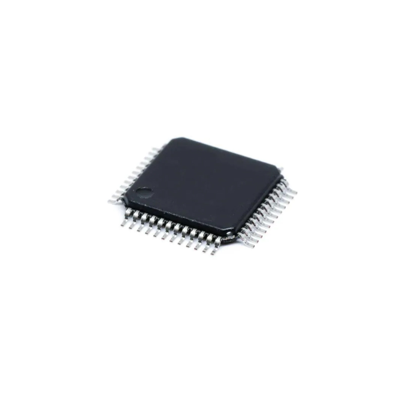
$5000C8051F332
8051 25 MHz 4 kB LFO 8-bit MCU


C8051F332 概要
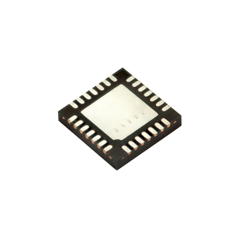
System OverviewC8051F330/1/2/3/4/5 devices are fully integrated mixed-signal System-on-a-Chip MCUs. Highlighted features are listed below. Refer to Table 1.1 for specific product feature selection.• High-speed pipelined 8051-compatible microcontroller core (up to 25 MIPS)• In-system, full-speed, non-intrusive debug interface (on-chip)• True 10-bit 200 ksps 16-channel single-ended/differential ADC with analog multiplexer• 10-bit Current Output DAC• Precision programmable 25 MHz internal oscillator• Up to 8 kB of on-chip Flash memory—512 bytes are reserved• 768 bytes of on-chip RAM• SMBus/I2C, Enhanced UART, and Enhanced SPI serial interfaces implemented in hardware• Four general-purpose 16-bit timers• Programmable Counter/Timer Array (PCA) with three capture/compare modules and Watchdog Timer function• On-chip Power-On Reset, VDD Monitor, and Temperature Sensor• On-chip Voltage Comparator• 17 Port I/O (5 V tolerant)Analog Peripherals - 10-Bit ADC (‘F330/2/4 only) • Up to 200 ksps • Up to 16 external single-ended or differential inputs • VREF from internal VREF, external pin or VDD • Internal or external start of conversion source • Built-in temperature sensor - 10-Bit Current Output DAC (‘F330 only) - Comparator • Programmable hysteresis and response time • Configurable as interrupt or reset source • Low current (0.4 µA)On-Chip Debug - On-chip debug circuitry facilitates full speed, nonintrusive in-system debug (no emulator required) - Provides breakpoints, single stepping, inspect/modify memory and registers - Superior performance to emulation systems using ICE-chips, target pods, and sockets - Low cost, complete development kitSupply Voltage 2.7 to 3.6 V - Typical operating current: 6.4 mA at 25 MHz; 9 µA at 32 kHz - Typical stop mode current: 0.1 µATemperature Range: –40 to +85 °CHigh Speed 8051 µC Core - Pipelined instruction architecture; executes 70% of instructions in 1 or 2 system clocks - Up to 25 MIPS throughput with 25 MHz clock - Expanded interrupt handler Memory - 768 bytes internal data RAM (256 + 512) - 8 kB (‘F330/1), 4 kB (‘F332/3), or 2 kB (‘F334/5) Flash; In-system programmable in 512-byte Sectors—512 bytes are reserved in the 8 kB devicesDigital Peripherals - 17 Port I/O; All 5 V tolerant with high sink current - Hardware enhanced UART, SMBus™, and enhanced SPI™ serial ports - Four general purpose 16-bit counter/timers - 16-Bit programmable counter array (PCA) with three capture/compare modules - Real time clock mode using PCA or timer and external clock sourceClock Sources - Two internal oscillators: • 24.5 MHz with ±2% accuracy supports crystal-less UART operation • 80/40/20/10 kHz low frequency, low power - External oscillator: Crystal, RC, C, or clock (1 or 2 pin modes) - Can switch between clock sources on-the-fly; useful in power saving modes20-Pin QFN Package
仕様
| パラメータ | 価値 | パラメータ | 価値 |
|---|---|---|---|
| EU RoHS | Compliant | ECCN (US) | EAR99 |
| Part Status | Active | HTS | 8542.31.00.01 |
| Automotive | No | PPAP | No |
| Family Name | C8051F33x | Instruction Set Architecture | CISC |
| Device Core | 8051 | Core Architecture | 8051 |
| Maximum CPU Frequency (MHz) | 25 | Maximum Clock Rate (MHz) | 25 |
| Data Bus Width (bit) | 8 | Program Memory Type | Flash |
| Program Memory Size | 4KB | RAM Size | 768B |
| Maximum Expanded Memory Size | 64KB | Programmability | Yes |
| Interface Type | I2C/SMBus/SPI/UART | Number of I/Os | 17 |
| No. of Timers | 4 | Timers Resolution (bit) | 16/16/16/16 |
| PWM | 3 | Number of ADCs | Single |
| ADC Channels | 16 | ADC Resolution (bit) | 10 |
| USART | 0 | UART | 1 |
| USB | 0 | SPI | 1 |
| I2C | 1 | I2S | 0 |
| CAN | 0 | Ethernet | 0 |
| Watchdog | 1 | Analog Comparators | 1 |
| Parallel Master Port | No | Real Time Clock | Yes |
| Special Features | Programmable Counter Array | Minimum Operating Supply Voltage (V) | 2.7 |
| Typical Operating Supply Voltage (V) | 3.3 | Maximum Operating Supply Voltage (V) | 3.6 |
| Minimum Operating Temperature (°C) | -40 | Maximum Operating Temperature (°C) | 85 |
| Supplier Temperature Grade | Industrial | Packaging | Tube |
| Mounting | Surface Mount | Package Height | 0.88 |
| Package Width | 4 | Package Length | 4 |
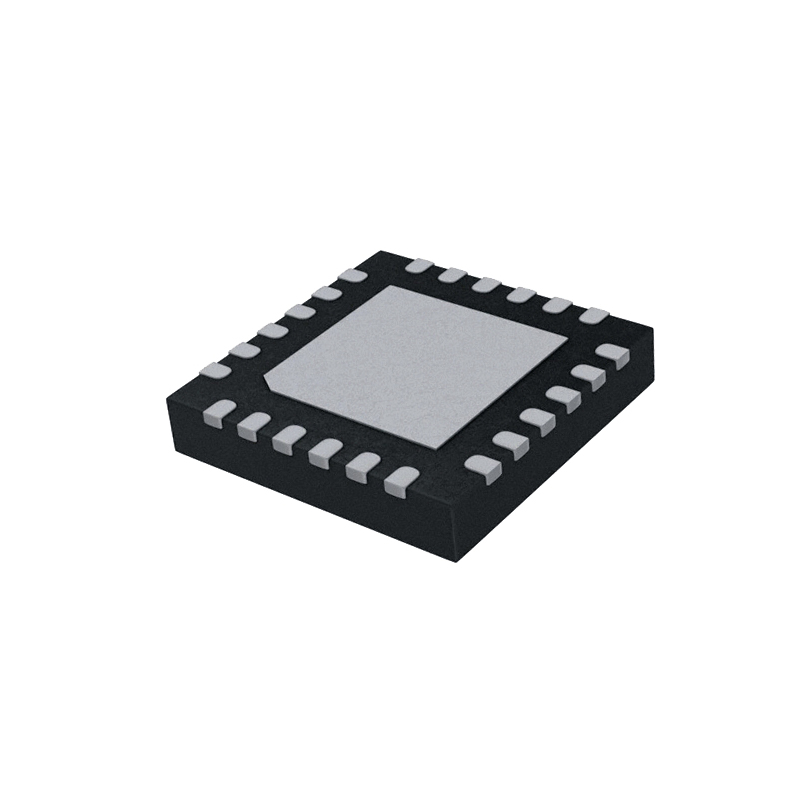
| PCB changed | 20 | Standard Package Name | QFN |
| Supplier Package | QFN | Pin Count | 20 |
| Lead Shape | No Lead |
配送
| 配送タイプ | 配送料 | リードタイム | |
|---|---|---|---|
 |
DHL | $20.00-$40.00 (0.50 KG) | 2-5 日々 |
 |
フェデックス | $20.00-$40.00 (0.50 KG) | 2-5 日々 |
 |
UPS | $20.00-$40.00 (0.50 KG) | 2-5 日々 |
 |
TNT | $20.00-$40.00 (0.50 KG) | 2-5 日々 |
 |
EMS | $20.00-$40.00 (0.50 KG) | 2-5 日々 |
 |
登録された航空便 | $20.00-$40.00 (0.50 KG) | 2-5 日々 |
処理時間:送料は地域や国によって異なります。
支払い
| 支払条件 | ハンドフィー | |
|---|---|---|
 |
電信送金 | 銀行手数料 US$30.00 を請求します。 |
 |
ペイパル | 4.0%のサービス料がかかります。 |
 |
クレジットカード | 3.5%のサービス料がかかります。 |
 |
ウエスタンユニオン | charge US.00 banking fee. |
 |
送金サービス | 銀行手数料は 0.00 米ドルかかります。 |
保証
1.購入した電子部品には365日保証が含まれており、製品の品質を保証します。
2.受け取った商品の一部が完璧な品質ではない場合、当社は責任を持って返金または交換を手配します。 ただし、商品は元の状態のままでなければなりません。
パッキング
-

ステップ1 :製品
-

ステップ2 :真空包装
-

ステップ3 :静電気防止袋
-

ステップ4 :個包装
-

ステップ5 :梱包箱
-

ステップ6 :バーコード配送タグ


すべての製品は静電気防止袋に梱包されます。 ESD 帯電防止保護を備えた状態で出荷されます。
社外の ESD 梱包ラベルには、部品番号、ブランド、数量などの当社の情報が使用されます。
私たちは出荷前にすべての商品を検査し、すべての製品が良好な状態であることを確認し、部品が新しいオリジナルでデータシートと一致していることを確認します。
すべての商品に問題がないことを確認した後、梱包後、安全に梱包し、グローバルエクスプレスで発送します。 優れた耐穿刺性と耐引裂性を示し、シールの完全性も良好です。


私たちは高品質の製品、思いやりのあるサービス、販売後の保証を提供します
-

豊富な商品を取り揃えておりますので、お客様の様々なニーズにお応え致します。
-

最小注文数量は1個からとなります。
-

最低国際配送料は0.00ドルから
-

全商品365日品質保証


