画像は参考用です。製品仕様を参照してください。
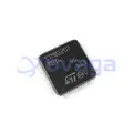
AM3352BZCZ80

Microprocessors - MPU Sitara ARM Cortex-A8 MPU


ブランド: TEXAS INSTRUMENTS INC
製造元部品 #: AM3352BZCZ80
データシート: AM3352BZCZ80 データシート (PDF)
パッケージ/ケース: PBGA-324
RoHS ステータス:
在庫状況: 6778 個、新しいオリジナル
製品の種類: Microprocessors - MPU
Warranty: 1 Year Ovaga Warranty - Find Out More
0
1
*すべての価格は米ドルです
| 数量 | 単価 | 外部価格 |
|---|---|---|
| 1 | $10.323 | $10.323 |
| 10 | $9.043 | $90.430 |
| 30 | $8.261 | $247.830 |
| 100 | $7.609 | $760.900 |
In Stock:6778 PCS
AM3352BZCZ80 概要
The AM335x microprocessors, based on the ARM Cortex-A8 processor, are enhanced with image, graphics processing, peripherals and industrial interface options such as EtherCAT and PROFIBUS. The devices support high-level operating systems (HLOS). Processor SDK Linux® and TI-RTOS are available free of charge from TI.
The AM335x microprocessor contains the subsystems shown in the Functional Block Diagram and a brief description of each follows:
The contains the subsystems shown in the Functional Block Diagram and a brief description of each follows:
The microprocessor unit (MPU) subsystem is based on the ARM Cortex-A8 processor and the PowerVR SGX™ Graphics Accelerator subsystem provides 3D graphics acceleration to support display and gaming effects.
The PRU-ICSS is separate from the ARM core, allowing independent operation and clocking for greater efficiency and flexibility. The PRU-ICSS enables additional peripheral interfaces and real-time protocols such as EtherCAT, PROFINET, EtherNet/IP, PROFIBUS, Ethernet Powerlink, Sercos, and others. Additionally, the programmable nature of the PRU-ICSS, along with its access to pins, events and all system-on-chip (SoC) resources, provides flexibility in implementing fast, real-time responses, specialized data handling operations, custom peripheral interfaces, and in offloading tasks from the other processor cores of SoC.
特徴
- Up to 1-GHz Sitara™ ARM® Cortex®-A8 32‑Bit RISC Processor
- NEON™ SIMD Coprocessor
- 32KB of L1 Instruction and 32KB of Data Cache With Single-Error Detection (Parity)
- 256KB of L2 Cache With Error Correcting Code (ECC)
- 176KB of On-Chip Boot ROM
- 64KB of Dedicated RAM
- Emulation and Debug - JTAG
- Interrupt Controller (up to 128 Interrupt Requests)
- On-Chip Memory (Shared L3 RAM)
- 64KB of General-Purpose On-Chip Memory Controller (OCMC) RAM
- Accessible to All Masters
- Supports Retention for Fast Wakeup
- External Memory Interfaces (EMIF)
- mDDR(LPDDR), DDR2, DDR3, DDR3L Controller:
- mDDR: 200-MHz Clock (400-MHz Data Rate)
- DDR2: 266-MHz Clock (532-MHz Data Rate)
- DDR3: 400-MHz Clock (800-MHz Data Rate)
- DDR3L: 400-MHz Clock (800-MHz Data Rate)
- 16-Bit Data Bus
- 1GB of Total Addressable Space
- Supports One x16 or Two x8 Memory Device Configurations
- General-Purpose Memory Controller (GPMC)
- Flexible 8-Bit and 16-Bit Asynchronous Memory Interface With up to Seven Chip Selects (NAND, NOR, Muxed-NOR, SRAM)
- Uses BCH Code to Support 4-, 8-, or 16-Bit ECC
- Uses Hamming Code to Support 1-Bit ECC
- Error Locator Module (ELM)
- Used in Conjunction With the GPMC to Locate Addresses of Data Errors from Syndrome Polynomials Generated Using a BCH Algorithm
- Supports 4-, 8-, and 16-Bit per 512-Byte Block Error Location Based on BCH Algorithms
- mDDR(LPDDR), DDR2, DDR3, DDR3L Controller:
- Programmable Real-Time Unit Subsystem and Industrial Communication Subsystem (PRU-ICSS)
- Supports Protocols such as EtherCAT®, PROFIBUS, PROFINET, EtherNet/IP™, and More
- Two Programmable Real-Time Units (PRUs)
- 32-Bit Load/Store RISC Processor Capable of Running at 200 MHz
- 8KB of Instruction RAM With Single-Error Detection (Parity)
- 8KB of Data RAM With Single-Error Detection (Parity)
- Single-Cycle 32-Bit Multiplier With 64-Bit Accumulator
- Enhanced GPIO Module Provides Shift-In/Out Support and Parallel Latch on External Signal
- 12KB of Shared RAM With Single-Error Detection (Parity)
- Three 120-Byte Register Banks Accessible by Each PRU
- Interrupt Controller (INTC) for Handling System Input Events
- Local Interconnect Bus for Connecting Internal and External Masters to the Resources Inside the PRU-ICSS
- Peripherals Inside the PRU-ICSS:
- One UART Port With Flow Control Pins, Supports up to 12 Mbps
- One Enhanced Capture (eCAP) Module
- Two MII Ethernet Ports that Support Industrial Ethernet, such as EtherCAT
- One MDIO Port
- Power, Reset, and Clock Management (PRCM) Module
- Controls the Entry and Exit of Stand-By and Deep-Sleep Modes
- Responsible for Sleep Sequencing, Power Domain Switch-Off Sequencing, Wake-Up Sequencing, and Power Domain Switch-On Sequencing
- Clocks
- Integrated 15- to 35-MHz High-Frequency Oscillator Used to Generate a Reference Clock for Various System and Peripheral Clocks
- Supports Individual Clock Enable and Disable Control for Subsystems and Peripherals to Facilitate Reduced Power Consumption
- Five ADPLLs to Generate System Clocks (MPU Subsystem, DDR Interface, USB and Peripherals [MMC and SD, UART, SPI, I2C], L3, L4, Ethernet, GFX [SGX530], LCD Pixel Clock)
- Power
- Two Nonswitchable Power Domains (Real-Time Clock [RTC], Wake-Up Logic [WAKEUP])
- Three Switchable Power Domains (MPU Subsystem [MPU], SGX530 [GFX], Peripherals and Infrastructure [PER])
- Implements SmartReflex™ Class 2B for Core Voltage Scaling Based On Die Temperature, Process Variation, and Performance (Adaptive Voltage Scaling [AVS])
- Dynamic Voltage Frequency Scaling (DVFS)
- Real-Time Clock (RTC)
- Real-Time Date (Day-Month-Year-Day of Week) and Time (Hours-Minutes-Seconds) Information
- Internal 32.768-kHz Oscillator, RTC Logic and 1.1-V Internal LDO
- Independent Power-on-Reset (RTC_PWRONRSTn) Input
- Dedicated Input Pin (EXT_WAKEUP) for External Wake Events
- Programmable Alarm Can be Used to Generate Internal Interrupts to the PRCM (for Wakeup) or Cortex-A8 (for Event Notification)
- Programmable Alarm Can be Used With External Output (PMIC_POWER_EN) to Enable the Power Management IC to Restore Non-RTC Power Domains
- Peripherals
- Up to Two USB 2.0 High-Speed DRD (Dual-Role Device) Ports With Integrated PHY
- Up to Two Industrial Gigabit Ethernet MACs (10, 100, 1000 Mbps)
- Integrated Switch
- Each MAC Supports MII, RMII, RGMII, and MDIO Interfaces
- Ethernet MACs and Switch Can Operate Independent of Other Functions
- IEEE 1588v1 Precision Time Protocol (PTP)
- Up to Two Controller-Area Network (CAN) Ports
- Supports CAN Version 2 Parts A and B
- Up to Two Multichannel Audio Serial Ports (McASPs)
- Transmit and Receive Clocks up to 50 MHz
- Up to Four Serial Data Pins per McASP Port With Independent TX and RX Clocks
- Supports Time Division Multiplexing (TDM), Inter-IC Sound (I2S), and Similar Formats
- Supports Digital Audio Interface Transmission (SPDIF, IEC60958-1, and AES-3 Formats)
- FIFO Buffers for Transmit and Receive (256 Bytes)
- Up to Six UARTs
- All UARTs Support IrDA and CIR Modes
- All UARTs Support RTS and CTS Flow Control
- UART1 Supports Full Modem Control
- Up to Two Master and Slave McSPI Serial Interfaces
- Up to Two Chip Selects
- Up to 48 MHz
- Up to Three MMC, SD, SDIO Ports
- 1-, 4- and 8-Bit MMC, SD, SDIO Modes
- MMCSD0 has Dedicated Power Rail for 1.8‑V or 3.3-V Operation
- Up to 48-MHz Data Transfer Rate
- Supports Card Detect and Write Protect
- Complies With MMC4.3, SD, SDIO 2.0 Specifications
- Up to Three I2C Master and Slave Interfaces
- Standard Mode (up to 100 kHz)
- Fast Mode (up to 400 kHz)
- Up to Four Banks of General-Purpose I/O (GPIO) Pins
- 32 GPIO Pins per Bank (Multiplexed With Other Functional Pins)
- GPIO Pins Can be Used as Interrupt Inputs (up to Two Interrupt Inputs per Bank)
- Up to Three External DMA Event Inputs that can Also be Used as Interrupt Inputs
- Eight 32-Bit General-Purpose Timers
- DMTIMER1 is a 1-ms Timer Used for Operating System (OS) Ticks
- DMTIMER4–DMTIMER7 are Pinned Out
- One Watchdog Timer
- SGX530 3D Graphics Engine
- Tile-Based Architecture Delivering up to 20 Million Polygons per Second
- Universal Scalable Shader Engine (USSE) is a Multithreaded Engine Incorporating Pixel and Vertex Shader Functionality
- Advanced Shader Feature Set in Excess of Microsoft VS3.0, PS3.0, and OGL2.0
- Industry Standard API Support of Direct3D Mobile, OGL-ES 1.1 and 2.0, and OpenMax
- Fine-Grained Task Switching, Load Balancing, and Power Management
- Advanced Geometry DMA-Driven Operation for Minimum CPU Interaction
- Programmable High-Quality Image Anti-Aliasing
- Fully Virtualized Memory Addressing for OS Operation in a Unified Memory Architecture
- LCD Controller
- Up to 24-Bit Data Output; 8 Bits per Pixel (RGB)
- Resolution up to 2048 × 2048 (With Maximum 126-MHz Pixel Clock)
- Integrated LCD Interface Display Driver (LIDD) Controller
- Integrated Raster Controller
- Integrated DMA Engine to Pull Data from the External Frame Buffer Without Burdening the Processor via Interrupts or a Firmware Timer
- 512-Word Deep Internal FIFO
- Supported Display Types:
- Character Displays - Uses LIDD Controller to Program these Displays
- Passive Matrix LCD Displays - Uses LCD Raster Display Controller to Provide Timing and Data for Constant Graphics Refresh to a Passive Display
- Active Matrix LCD Displays - Uses External Frame Buffer Space and the Internal DMA Engine to Drive Streaming Data to the Panel
- 12-Bit Successive Approximation Register (SAR) ADC
- 200K Samples per Second
- Input can be Selected from any of the Eight Analog Inputs Multiplexed Through an 8:1 Analog Switch
- Can be Configured to Operate as a 4-Wire, 5-Wire, or 8-Wire Resistive Touch Screen Controller (TSC) Interface
- Up to Three 32-Bit eCAP Modules
- Configurable as Three Capture Inputs or Three Auxiliary PWM Outputs
- Up to Three Enhanced High-Resolution PWM Modules (eHRPWMs)
- Dedicated 16-Bit Time-Base Counter With Time and Frequency Controls
- Configurable as Six Single-Ended, Six Dual-Edge Symmetric, or Three Dual-Edge Asymmetric Outputs
- Up to Three 32-Bit Enhanced Quadrature Encoder Pulse (eQEP) Modules
- Device Identification
- Contains Electrical Fuse Farm (FuseFarm) of Which Some Bits are Factory Programmable
- Production ID
- Device Part Number (Unique JTAG ID)
- Device Revision (Readable by Host ARM)
- Contains Electrical Fuse Farm (FuseFarm) of Which Some Bits are Factory Programmable
- Debug Interface Support
- JTAG and cJTAG for ARM (Cortex-A8 and PRCM), PRU-ICSS Debug
- Supports Device Boundary Scan
- Supports IEEE 1500
- DMA
- On-Chip Enhanced DMA Controller (EDMA) has Three Third-Party Transfer Controllers (TPTCs) and One Third-Party Channel Controller (TPCC), Which Supports up to 64 Programmable Logical Channels and Eight QDMA Channels. EDMA is Used for:
- Transfers to and from On-Chip Memories
- Transfers to and from External Storage (EMIF, GPMC, Slave Peripherals)
- On-Chip Enhanced DMA Controller (EDMA) has Three Third-Party Transfer Controllers (TPTCs) and One Third-Party Channel Controller (TPCC), Which Supports up to 64 Programmable Logical Channels and Eight QDMA Channels. EDMA is Used for:
- Inter-Processor Communication (IPC)
- Integrates Hardware-Based Mailbox for IPC and Spinlock for Process Synchronization Between Cortex-A8, PRCM, and PRU-ICSS
- Mailbox Registers that Generate Interrupts
- Four Initiators (Cortex-A8, PRCM, PRU0, PRU1)
- Spinlock has 128 Software-Assigned Lock Registers
- Mailbox Registers that Generate Interrupts
- Integrates Hardware-Based Mailbox for IPC and Spinlock for Process Synchronization Between Cortex-A8, PRCM, and PRU-ICSS
- Security
- Crypto Hardware Accelerators (AES, SHA, RNG)
- Secure Boot (optional; requires custom part engagement with TI)
- Boot Modes
- Boot Mode is Selected Through Boot Configuration Pins Latched on the Rising Edge of the PWRONRSTn Reset Input Pin
- Packages:
- 298-Pin S-PBGA-N298 Via Channel Package
(ZCE Suffix), 0.65-mm Ball Pitch - 324-Pin S-PBGA-N324 Package
(ZCZ Suffix), 0.80-mm Ball Pitch
- 298-Pin S-PBGA-N298 Via Channel Package
仕様
| パラメータ | 価値 | パラメータ | 価値 |
|---|---|---|---|
| Source Content uid | AM3352BZCZ80 | Pbfree Code | Yes |
| Rohs Code | Yes | Part Life Cycle Code | Active |
| Ihs Manufacturer | TEXAS INSTRUMENTS INC | Package Description | NFBGA-324 |
| Reach Compliance Code | compliant | ECCN Code | 5A992.C |
| HTS Code | 8542.31.00.01 | Samacsys Manufacturer | Texas Instruments |
| Address Bus Width | 28 | Bit Size | 32 |
| Boundary Scan | YES | External Data Bus Width | 16 |
| Format | FIXED POINT | Integrated Cache | YES |
| JESD-30 Code | S-PBGA-B324 | Low Power Mode | YES |
| Moisture Sensitivity Level | 3 | Number of DMA Channels | 64 |
| Number of Terminals | 324 | On Chip Data RAM Width | 8 |
| Package Body Material | PLASTIC/EPOXY | Package Code | LFBGA |
| Package Equivalence Code | BGA324,18X18,32 | Package Shape | SQUARE |
| Package Style | GRID ARRAY, LOW PROFILE, FINE PITCH | Peak Reflow Temperature (Cel) | 260 |
| RAM (words) | 131072 | Surface Mount | YES |
| Technology | CMOS | Temperature Grade | OTHER |
| Terminal Finish | TIN SILVER COPPER | Terminal Form | BALL |
| Terminal Position | BOTTOM | Time@Peak Reflow Temperature-Max (s) | 30 |
| uPs/uCs/Peripheral ICs Type | MICROPROCESSOR, RISC |
配送
| 配送タイプ | 配送料 | リードタイム | |
|---|---|---|---|
 |
DHL | $20.00-$40.00 (0.50 KG) | 2-5 日々 |
 |
フェデックス | $20.00-$40.00 (0.50 KG) | 2-5 日々 |
 |
UPS | $20.00-$40.00 (0.50 KG) | 2-5 日々 |
 |
TNT | $20.00-$40.00 (0.50 KG) | 2-5 日々 |
 |
EMS | $20.00-$40.00 (0.50 KG) | 2-5 日々 |
 |
登録された航空便 | $20.00-$40.00 (0.50 KG) | 2-5 日々 |
処理時間:送料は地域や国によって異なります。
支払い
| 支払条件 | ハンドフィー | |
|---|---|---|
 |
電信送金 | 銀行手数料 US$30.00 を請求します。 |
 |
ペイパル | 4.0%のサービス料がかかります。 |
 |
クレジットカード | 3.5%のサービス料がかかります。 |
 |
ウエスタンユニオン | charge US.00 banking fee. |
 |
送金サービス | 銀行手数料は 0.00 米ドルかかります。 |
保証
1.購入した電子部品には365日保証が含まれており、製品の品質を保証します。
2.受け取った商品の一部が完璧な品質ではない場合、当社は責任を持って返金または交換を手配します。 ただし、商品は元の状態のままでなければなりません。
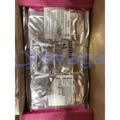
パッキング
-

ステップ1 :製品
-

ステップ2 :真空包装
-

ステップ3 :静電気防止袋
-

ステップ4 :個包装
-

ステップ5 :梱包箱
-

ステップ6 :バーコード配送タグ


すべての製品は静電気防止袋に梱包されます。 ESD 帯電防止保護を備えた状態で出荷されます。
社外の ESD 梱包ラベルには、部品番号、ブランド、数量などの当社の情報が使用されます。
私たちは出荷前にすべての商品を検査し、すべての製品が良好な状態であることを確認し、部品が新しいオリジナルでデータシートと一致していることを確認します。
すべての商品に問題がないことを確認した後、梱包後、安全に梱包し、グローバルエクスプレスで発送します。 優れた耐穿刺性と耐引裂性を示し、シールの完全性も良好です。


パーツポイント
-
The AM3352BZCZ80 is a system-on-chip (SoC) from Texas Instruments, part of the Sitara family. It features an ARM Cortex-A8 processor with speeds up to 800MHz, along with various peripherals and connectivity options. The chip is commonly used in embedded systems, IoT devices, industrial automation, and more.
-
Equivalent
Some equivalent products of the AM3352BZCZ80 chip are: 1. AM3352BZCE30 2. AM3352BZCZ60 3. AM3352BZCZD30 These chips are part of the Sitara AM335x family of embedded processors and offer similar performance and features to the AM3352BZCZ80 chip. -
Features
AM3352BZCZ80 features a 32-bit ARM Cortex-A8 processor running at up to 1 GHz, 512 MB DDR3 RAM, dual PRUs, Gigabit Ethernet, USB 2.0 ports, multiple serial communication interfaces, 200-pin SODIMM connector, and industrial temperature range support. -
Pinout
The AM3352BZCZ80 is a 484-ball BGA package with a 0.65mm pitch. It is a system-on-chip (SoC) designed for embedded applications, with a dual-core ARM Cortex-A8 processor, 3D graphics accelerator, and various peripherals. Key functions include control of GPIO, UART, I2C, SPI interfaces, and support for Ethernet, USB, and audio interfaces. -
Manufacturer
The manufacturer of the AM3352BZCZ80 is Texas Instruments. Texas Instruments is a multinational semiconductor manufacturing company known for its extensive range of semiconductor products for various applications including analog, embedded processing, and wireless connectivity solutions. -
Application Field
The AM3352BZCZ80 is commonly used in industrial automation, smart grid, home automation, and portable data terminals due to its low power consumption, integrated peripherals, and processing capabilities. It is also used in consumer electronics such as fitness trackers, wearables, and smart appliances. -
Package
The AM3352BZCZ80 chip comes in a 760-Ball BGA package, with a size of 17x17mm.


私たちは高品質の製品、思いやりのあるサービス、販売後の保証を提供します
-

豊富な商品を取り揃えておりますので、お客様の様々なニーズにお応え致します。
-

最小注文数量は1個からとなります。
-

最低国際配送料は0.00ドルから
-

全商品365日品質保証