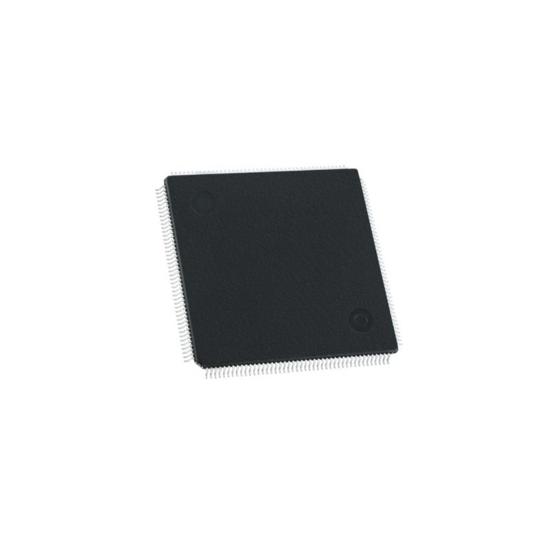
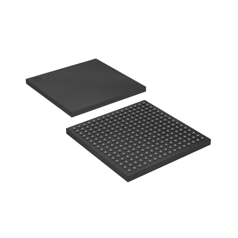
画像は参考用です。製品仕様を参照してください。
注文金額が
$5000AGL125V2-FGG144I
Supports innovative circuit development and testin


ブランド: MICROCHIP TECHNOLOGY INC
製造元部品 #: AGL125V2-FGG144I
データシート: AGL125V2-FGG144I データシート (PDF)
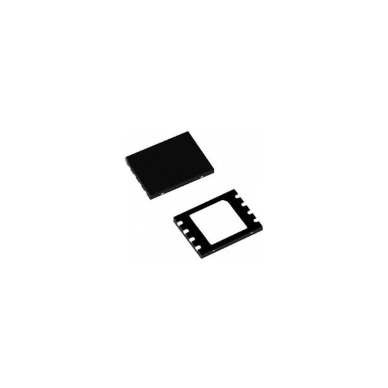
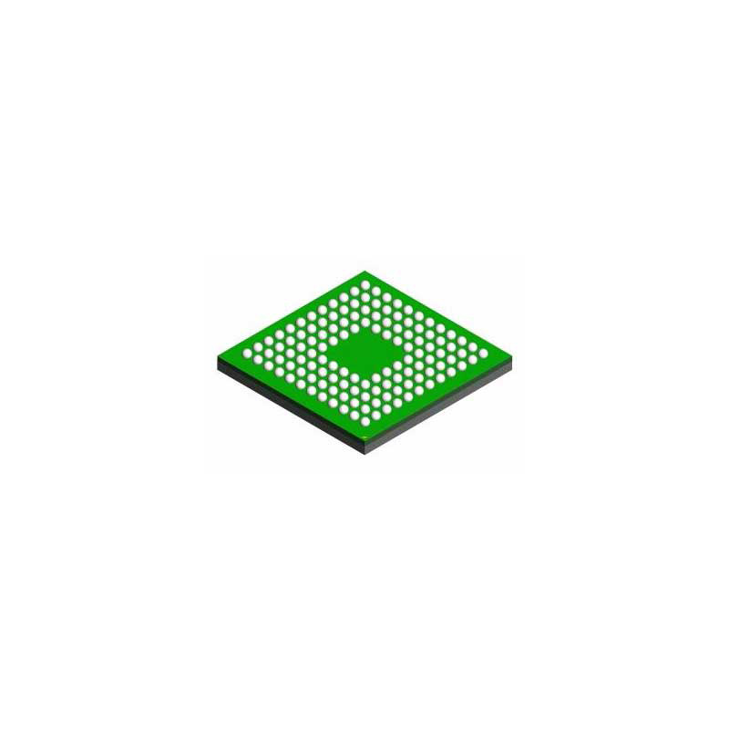
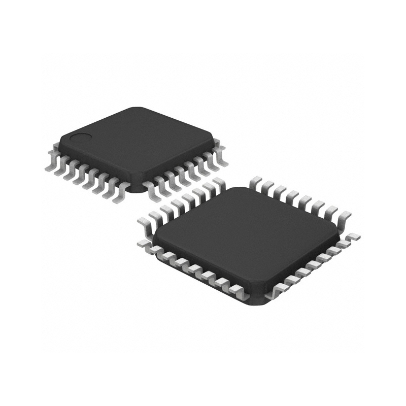
パッケージ/ケース: 144-FPBGA (13x13)
AGL125V2-FGG144I 概要
This FPGA is specifically engineered for applications demanding high performance and low power consumption, including industrial control, automotive, communication systems, and aerospace. Its programmability using a range of design tools and support for industry-standard interfaces like JTAG and SPI for configuration, further enhances its usability in diverse projects
特徴
- Low Power
- 1.2 V to 1.5 V Core Voltage Support for Low Power
- Supports Single-Voltage System Operation
- 5 µW Power Consumption in FlashFreeze Mode
- Low Power Active FPGA Operation
- FlashFreeze Technology Enables Ultra-Low Power Consumption while Maintaining FPGA Content
- Easy Entry to / Exit from Ultra-Low Power FlashFreeze Mode
仕様
| パラメータ | 価値 | パラメータ | 価値 |
|---|---|---|---|
| Rohs Code | Yes | Part Life Cycle Code | Active |
| Ihs Manufacturer | MICROCHIP TECHNOLOGY INC | Package Description | 13 X 13 MM, 1.45 MM HEIGHT, 1 MM PITCH, HALOGEN FREE AND ROHS COMPLIANT, FBGA-144 |
| Reach Compliance Code | compliant | HTS Code | 8542.39.00.01 |
| JESD-30 Code | S-PBGA-B144 | JESD-609 Code | e1 |
| Length | 13 mm | Moisture Sensitivity Level | 3 |
| Number of Equivalent Gates | 125000 | Number of Inputs | 97 |
| Number of Logic Cells | 3072 | Number of Outputs | 97 |
| Number of Terminals | 144 | Operating Temperature-Max | 100 °C |
| Operating Temperature-Min | -40 °C | Organization | 125000 GATES |
| Package Body Material | PLASTIC/EPOXY | Package Code | LBGA |
| Package Equivalence Code | BGA144,12X12,40 | Package Shape | SQUARE |
| Package Style | GRID ARRAY, LOW PROFILE | Peak Reflow Temperature (Cel) | 260 |
| Programmable Logic Type | FIELD PROGRAMMABLE GATE ARRAY | Qualification Status | Not Qualified |
| Seated Height-Max | 1.55 mm | Supply Voltage-Max | 1.575 V |
| Supply Voltage-Min | 1.14 V | Supply Voltage-Nom | 1.2 V |
| Surface Mount | YES | Technology | CMOS |
| Temperature Grade | INDUSTRIAL | Terminal Finish | TIN SILVER COPPER |
| Terminal Form | BALL | Terminal Pitch | 1 mm |
| Terminal Position | BOTTOM | Time@Peak Reflow Temperature-Max (s) | 30 |
| Width | 13 mm |
配送
| 配送タイプ | 配送料 | リードタイム | |
|---|---|---|---|
 |
DHL | $20.00-$40.00 (0.50 KG) | 2-5 日々 |
 |
フェデックス | $20.00-$40.00 (0.50 KG) | 2-5 日々 |
 |
UPS | $20.00-$40.00 (0.50 KG) | 2-5 日々 |
 |
TNT | $20.00-$40.00 (0.50 KG) | 2-5 日々 |
 |
EMS | $20.00-$40.00 (0.50 KG) | 2-5 日々 |
 |
登録された航空便 | $20.00-$40.00 (0.50 KG) | 2-5 日々 |
処理時間:送料は地域や国によって異なります。
支払い
| 支払条件 | ハンドフィー | |
|---|---|---|
 |
電信送金 | 銀行手数料 US$30.00 を請求します。 |
 |
ペイパル | 4.0%のサービス料がかかります。 |
 |
クレジットカード | 3.5%のサービス料がかかります。 |
 |
ウエスタンユニオン | charge US.00 banking fee. |
 |
送金サービス | 銀行手数料は 0.00 米ドルかかります。 |
保証
1.購入した電子部品には365日保証が含まれており、製品の品質を保証します。
2.受け取った商品の一部が完璧な品質ではない場合、当社は責任を持って返金または交換を手配します。 ただし、商品は元の状態のままでなければなりません。
パッキング
-

ステップ1 :製品
-

ステップ2 :真空包装
-

ステップ3 :静電気防止袋
-

ステップ4 :個包装
-

ステップ5 :梱包箱
-

ステップ6 :バーコード配送タグ


すべての製品は静電気防止袋に梱包されます。 ESD 帯電防止保護を備えた状態で出荷されます。
社外の ESD 梱包ラベルには、部品番号、ブランド、数量などの当社の情報が使用されます。
私たちは出荷前にすべての商品を検査し、すべての製品が良好な状態であることを確認し、部品が新しいオリジナルでデータシートと一致していることを確認します。
すべての商品に問題がないことを確認した後、梱包後、安全に梱包し、グローバルエクスプレスで発送します。 優れた耐穿刺性と耐引裂性を示し、シールの完全性も良好です。


パーツポイント
-
The AGL125V2-FGG144I is a field-programmable gate array (FPGA) chip designed by Microchip Technology. It features 125,000 logic elements, 2.5 Mb of RAM, and 144-pin FineLine BGA packaging. This chip offers customizable hardware acceleration for a wide range of applications, from automotive to industrial to consumer electronics.
-
Equivalent
The equivalent products of AGL125V2-FGG144I chip are AGL125V2-FGG1156I, AGL125V2-FGG1156T, and AGL125V2-FGG1156P. These chips are all part of the AGL125V2 family of low-power FPGAs from Microchip. -
Features
The AGL125V2-FGG144I is an FPGA (Field Programmable Gate Array) with 125,000 logic cells, 3600 kbits of RAM, and 144 IO pins. It features low power consumption, high performance, and programmable logic functions for a wide range of applications such as industrial control, communications, and automotive systems. -
Pinout
AGL125V2-FGG144I is a Field-Programmable Gate Array (FPGA) with 144 pins in a Fine-Pitch Ball Grid Array (FBGA) package. It features 125,000 logic cells and is suitable for various applications including signal processing, image processing, and industrial automation. -
Manufacturer
The manufacturer of the AGL125V2-FGG144I is Avnet. Avnet is a global technology solutions company that provides design, distribution, and marketing services for electronic components and computer products. They cater to a wide range of industries including automotive, industrial, aerospace, and defense. -
Application Field
AGL125V2-FGG144I is commonly used in industrial automation, automotive systems, telecommunications, and medical devices. It is suitable for applications requiring high reliability, low power consumption, and compact size. -
Package
The AGL125V2-FGG144I chip is a Field Programmable Gate Array (FPGA) with a Ball Grid Array (BGA) package, containing 144 pins in a 13x13 grid, with a size of 14x14 mm.
私たちは高品質の製品、思いやりのあるサービス、販売後の保証を提供します
-

豊富な商品を取り揃えておりますので、お客様の様々なニーズにお応え致します。
-

最小注文数量は1個からとなります。
-

最低国際配送料は0.00ドルから
-

全商品365日品質保証