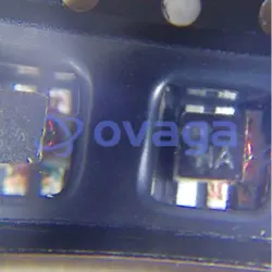
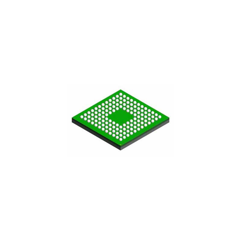
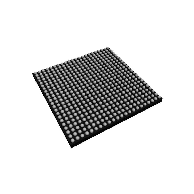
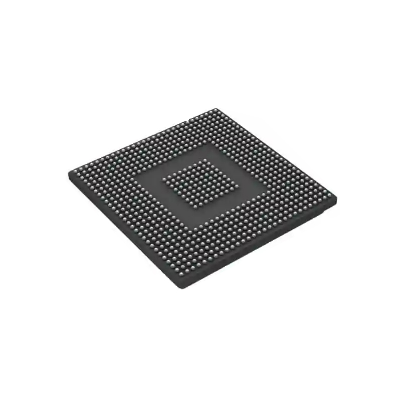
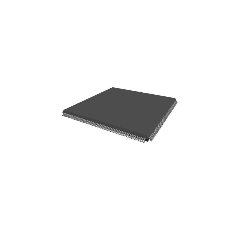
画像は参考用です。製品仕様を参照してください。
注文金額が
$5000A3P060-TQG144
0000 Gates, 1536 CLBs, 350MHz, Field Programmable Gate Array, CMOS, PQFP144


ブランド: MICROCHIP TECHNOLOGY INC
製造元部品 #: A3P060-TQG144
データシート: A3P060-TQG144 データシート (PDF)
パッケージ/ケース: TQFP-144
A3P060-TQG144 概要
Suitable for a variety of applications, the A3P060-TQG144 FPGA from Microchip Technology is part of the ProASIC3 family and comes in a TQG144 package. With 60,000 System Gates, 2880 Logic Cells, and 72 I/Os, this FPGA offers flexibility and customization for complex digital systems. Its 1 Mbit of embedded Flash memory eliminates the need for external memory components, reducing overall system cost. Operating at a maximum frequency of 250 MHz, the A3P060-TQG144 delivers high-speed performance for demanding applications
特徴
High Capacity 15 k to 1 M System Gates Up to 144 kbits of True Dual-Port SRAM Up to 300 User I/OsReprogrammable Flash Technology 130-nm, 7-Layer Metal (6 Copper), Flash-Based CMOS Process Instant On Level 0 Support Single-Chip Solution Retains Programmed Design when Powered OffHigh Performance 350 MHz System Performance 3.3 V, 66 MHz 64-Bit PCIIn-System Programming (ISP) and Security ISP Using On-Chip 128-Bit Advanced Encryption Standard (AES) Decryption (except ARM-enabled ProASIC3 devices) via JTAG (IEEE 1532compliant) FlashLock to Secure FPGA ContentsLow Power Core Voltage for Low Power Support for 1.5 V-Only Systems Low-Impedance Flash SwitchesHigh-Performance Routing Hierarchy Segmented, Hierarchical Routing and Clock StructureAdvanced I/O 700 Mbps DDR, LVDS-Capable I/Os (A3P250 and above) 1.5 V, 1.8 V, 2.5 V, and 3.3 V Mixed-Voltage Operation Wide Range Power Supply Voltage Support per JESD8-B, Allowing I/Os to Operate from 2.7 V to 3.6 V Bank-Selectable I/O Voltagesup to 4 Banks per Chip Single-Ended I/O Standards: LVTTL, LVCMOS 3.3 V / 2.5 V / 1.8 V / 1.5 V, 3.3 V PCI / 3.3 V PCI-X and LVCMOS 2.5 V / 5.0 V Input Differential I/O Standards: LVPECL, LVDS, B-LVDS, and M-LVDS (A3P250 and above) I/O Registers on Input, Output, and Enable Paths Hot-Swappable and Cold Sparing I/Os Programmable Output Slew Rate and Drive Strength Weak Pull-Up/-Down IEEE 1149.1 (JTAG) Boundary Scan Test Pin-Compatible Packages across the ProASIC3 FamilyClock Conditioning Circuit (CCC) and PLL Six CCC Blocks, One with an Integrated PLL Configurable Phase-Shift, Multiply/Divide, Delay Capabilities and External Feedback Wide Input Frequency Range (1.5 MHz to 350 MHz)Embedded Memory 1 kbit of FlashROM User Nonvolatile Memory SRAMs and FIFOs with Variable-Aspect-Ratio 4,608-Bit RAM Blocks (1, 2, 4, 9, and 18 organizations) True Dual-Port SRAM (except 18)ARM Processor Support in ProASIC3 FPGAs M1 ProASIC3 DevicesARMCortex-M1 Soft Processor Available with or without Debug
仕様
| パラメータ | 価値 | パラメータ | 価値 |
|---|---|---|---|
| Rohs Code | Yes | Part Life Cycle Code | Active |
| Ihs Manufacturer | MICROCHIP TECHNOLOGY INC | Package Description | 20 X 20 MM, 1.40 MM HEIGHT, 0.50 MM PITCH, GREEN, TQFP-144 |
| Reach Compliance Code | compliant | HTS Code | 8542.39.00.01 |
| Factory Lead Time | 52 Weeks | Clock Frequency-Max | 350 MHz |
| JESD-30 Code | S-PQFP-G144 | JESD-609 Code | e3 |
| Length | 20 mm | Moisture Sensitivity Level | 3 |
| Number of CLBs | 1536 | Number of Equivalent Gates | 60000 |
| Number of Terminals | 144 | Operating Temperature-Max | 85 °C |
| Operating Temperature-Min | Organization | 1536 CLBS, 60000 GATES | |
| Package Body Material | PLASTIC/EPOXY | Package Code | LFQFP |
| Package Shape | SQUARE | Package Style | FLATPACK, LOW PROFILE, FINE PITCH |
| Programmable Logic Type | FIELD PROGRAMMABLE GATE ARRAY | Qualification Status | Not Qualified |
| Seated Height-Max | 1.6 mm | Supply Voltage-Max | 1.575 V |
| Supply Voltage-Min | 1.425 V | Supply Voltage-Nom | 1.5 V |
| Surface Mount | YES | Technology | CMOS |
| Temperature Grade | COMMERCIAL | Terminal Finish | MATTE TIN |
| Terminal Form | GULL WING | Terminal Pitch | 0.5 mm |
| Terminal Position | QUAD |
配送
| 配送タイプ | 配送料 | リードタイム | |
|---|---|---|---|
 |
DHL | $20.00-$40.00 (0.50 KG) | 2-5 日々 |
 |
フェデックス | $20.00-$40.00 (0.50 KG) | 2-5 日々 |
 |
UPS | $20.00-$40.00 (0.50 KG) | 2-5 日々 |
 |
TNT | $20.00-$40.00 (0.50 KG) | 2-5 日々 |
 |
EMS | $20.00-$40.00 (0.50 KG) | 2-5 日々 |
 |
登録された航空便 | $20.00-$40.00 (0.50 KG) | 2-5 日々 |
処理時間:送料は地域や国によって異なります。
支払い
| 支払条件 | ハンドフィー | |
|---|---|---|
 |
電信送金 | 銀行手数料 US$30.00 を請求します。 |
 |
ペイパル | 4.0%のサービス料がかかります。 |
 |
クレジットカード | 3.5%のサービス料がかかります。 |
 |
ウエスタンユニオン | charge US.00 banking fee. |
 |
送金サービス | 銀行手数料は 0.00 米ドルかかります。 |
保証
1.購入した電子部品には365日保証が含まれており、製品の品質を保証します。
2.受け取った商品の一部が完璧な品質ではない場合、当社は責任を持って返金または交換を手配します。 ただし、商品は元の状態のままでなければなりません。
パッキング
-

ステップ1 :製品
-

ステップ2 :真空包装
-

ステップ3 :静電気防止袋
-

ステップ4 :個包装
-

ステップ5 :梱包箱
-

ステップ6 :バーコード配送タグ


すべての製品は静電気防止袋に梱包されます。 ESD 帯電防止保護を備えた状態で出荷されます。
社外の ESD 梱包ラベルには、部品番号、ブランド、数量などの当社の情報が使用されます。
私たちは出荷前にすべての商品を検査し、すべての製品が良好な状態であることを確認し、部品が新しいオリジナルでデータシートと一致していることを確認します。
すべての商品に問題がないことを確認した後、梱包後、安全に梱包し、グローバルエクスプレスで発送します。 優れた耐穿刺性と耐引裂性を示し、シールの完全性も良好です。


パーツポイント
-
The A3P060-TQG144 chip is a programmable logic device (PLD) from Actel/Microsemi that features 60,000 system gates and is housed in a 144-pin TQFP package. It offers a low-power, high-performance solution for a wide range of applications, including industrial automation, telecommunications, and consumer electronics.
-
Equivalent
Some equivalent products of the A3P060-TQG144 chip are XA3P060, A3P030, A3P060, A3P060-2VQG100, A3P060-2VQ100, and A3P060-2TQG144. These are all similar in terms of functionality, performance, and compatibility with different hardware and software systems. -
Features
A3P060-TQG144 is a flash-based, low power, and high reliability FPGA device. It offers 60,000 system gates with 144-pin TQFP package, and features FlashLock security, JTAG boundary scan, and programmable power management. It is suitable for a wide range of applications in industrial, automotive, and consumer markets. -
Pinout
A3P060-TQG144 is a flash-based FPGA with 144-pin TQFP package. It has 60 user I/O pins, along with various power, ground, and configuration pins. The function includes programmable logic functions, on-chip flash memory, and embedded 6051 processor core. -
Manufacturer
A3P060-TQG144 is manufactured by Microsemi Corporation, which is a leading provider of semiconductor solutions specializing in aerospace, defense, communications, and industrial markets. The company designs and produces high-performance and reliable integrated circuits for a wide range of applications, including FPGAs like the A3P060-TQG144. -
Application Field
A3P060-TQG144 is commonly used in various application areas such as industrial automation, automotive systems, telecommunications, and consumer electronics. It is ideal for applications requiring low power consumption, high performance, and compact size. This programmable logic device can be used for signal processing, motor control, data acquisition, and communication interfaces. -
Package
The A3P060-TQG144 chip has a Thin Quad Flat Pack (TQFP) package, with a form factor of 144 pins and a size of 14mm x 14mm.


私たちは高品質の製品、思いやりのあるサービス、販売後の保証を提供します
-

豊富な商品を取り揃えておりますので、お客様の様々なニーズにお応え致します。
-

最小注文数量は1個からとなります。
-

最低国際配送料は0.00ドルから
-

全商品365日品質保証