


画像は参考用です。製品仕様を参照してください。
注文金額が
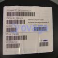
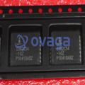
$5000Renesas 9FGV0841AKILF
Clock Generators & Support Products PCIE LOW POWER LOW VOLTAGE


ブランド: Renesas Technology Corp
製造元部品 #: 9FGV0841AKILF
データシート: 9FGV0841AKILF Datasheet (PDF)
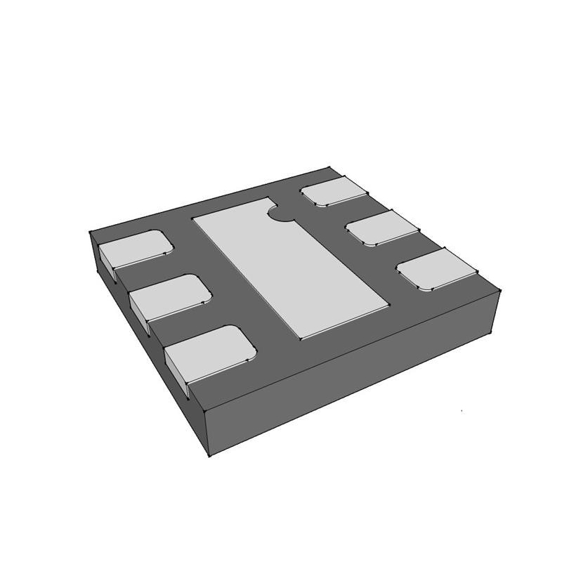
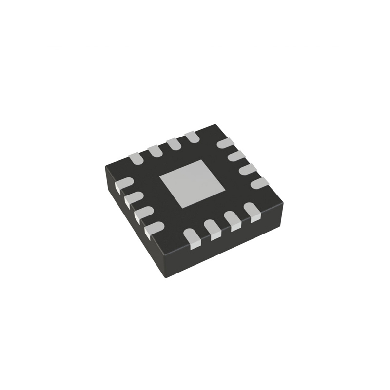
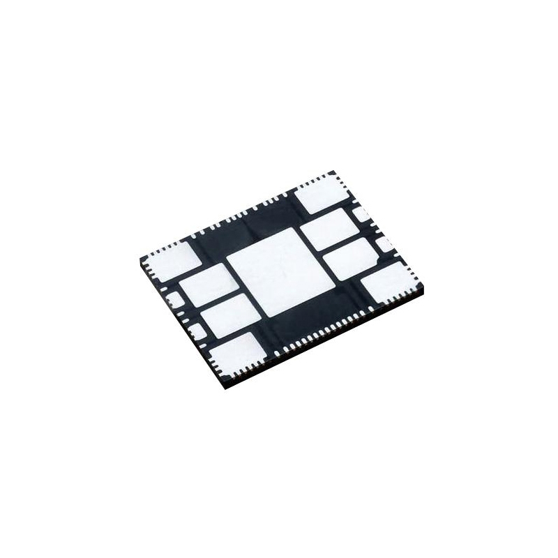
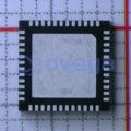
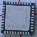
パッケージ/ケース: QFN-48
製品の種類: クロック&タイマIC
9FGV0841AKILF 概要
The 9FGV0841AKILF clock generator and buffer chip by IDT (now Renesas Electronics) is a versatile solution for demanding networking, computing, and data center environments. With its advanced design, this chip enables precise timing and synchronization crucial for high-performance systems. By providing multiple output clocks with minimal jitter, the 9FGV0841AKILF ensures seamless data transmission and coordination within the system. Its programmable output frequencies and low power consumption make it an efficient and reliable choice for a variety of applications. The chip is also compliant with industry standards like PCIe, SATA, and USB, offering seamless integration with existing systems. Designers can take advantage of the device's flexibility in clock synthesis and distribution to tailor performance to their specific needs, enhancing overall system efficiency. Compact and feature-rich, the 9FGV0841AKILF brings a new level of reliability and performance to complex electronic systems
特徴
- PCIe Gen1–4 compliant
- Integrated terminations provide 100Ω differential Zo: reduced component count and board space
- 1.8V operation: reduced power consumption
- Outputs can optionally be supplied from any voltage between 1.05V and 1.8V: maximum power savings
- OE# pins: support DIF power management
- LP-HCSL differential clock outputs: reduced power and board space
- Programmable slew rate for each output: allows tuning for various line lengths
- Programmable output amplitude: allows tuning for various application environments
- DIF outputs blocked until PLL is locked: clean system start-up
- Selectable 0%, -0.25% or -0.5% spread on DIF outputs: reduces EMI
- External 25MHz crystal; supports tight ppm with 0ppm synthesis error
- Configuration can be accomplished with strapping pins: SMBus interface not required for device control
- 3.3V tolerant SMBus interface works with legacy controllers
- Space-saving 6 × 6 mm 48-VFQFPN; minimal board space
- Selectable SMBus addresses: multiple devices can easily share an SMBus segment
- Available in AEC-Q100 qualified, Grade 2 (-40°C to +105°C) version (wettable flank package)
仕様
| パラメータ | 価値 | パラメータ | 価値 |
|---|---|---|---|
| Pin Count | 49 | Package Category | Quad Flat No-Lead |
| Released Date | May 10, 2018 |
配送
| 配送タイプ | 配送料 | リードタイム | |
|---|---|---|---|
 |
DHL | $20.00-$40.00 (0.50 KG) | 2-5 日々 |
 |
フェデックス | $20.00-$40.00 (0.50 KG) | 2-5 日々 |
 |
UPS | $20.00-$40.00 (0.50 KG) | 2-5 日々 |
 |
TNT | $20.00-$40.00 (0.50 KG) | 2-5 日々 |
 |
EMS | $20.00-$40.00 (0.50 KG) | 2-5 日々 |
 |
登録された航空便 | $20.00-$40.00 (0.50 KG) | 2-5 日々 |
処理時間:送料は地域や国によって異なります。
支払い
| 支払条件 | ハンドフィー | |
|---|---|---|
 |
電信送金 | 銀行手数料 US$30.00 を請求します。 |
 |
ペイパル | 4.0%のサービス料がかかります。 |
 |
クレジットカード | 3.5%のサービス料がかかります。 |
 |
ウエスタンユニオン | charge US.00 banking fee. |
 |
送金サービス | 銀行手数料は 0.00 米ドルかかります。 |
保証
1.購入した電子部品には365日保証が含まれており、製品の品質を保証します。
2.受け取った商品の一部が完璧な品質ではない場合、当社は責任を持って返金または交換を手配します。 ただし、商品は元の状態のままでなければなりません。
パッキング
-

ステップ1 :製品
-

ステップ2 :真空包装
-

ステップ3 :静電気防止袋
-

ステップ4 :個包装
-

ステップ5 :梱包箱
-

ステップ6 :バーコード配送タグ


すべての製品は静電気防止袋に梱包されます。 ESD 帯電防止保護を備えた状態で出荷されます。
社外の ESD 梱包ラベルには、部品番号、ブランド、数量などの当社の情報が使用されます。
私たちは出荷前にすべての商品を検査し、すべての製品が良好な状態であることを確認し、部品が新しいオリジナルでデータシートと一致していることを確認します。
すべての商品に問題がないことを確認した後、梱包後、安全に梱包し、グローバルエクスプレスで発送します。 優れた耐穿刺性と耐引裂性を示し、シールの完全性も良好です。


データシート PDF
私たちは高品質の製品、思いやりのあるサービス、販売後の保証を提供します
-

豊富な商品を取り揃えておりますので、お客様の様々なニーズにお応え致します。
-

最小注文数量は1個からとなります。
-

最低国際配送料は0.00ドルから
-

全商品365日品質保証


Efficient and reliable, Ovaga is my go-to provider for professional electronic components.