


画像は参考用です。製品仕様を参照してください。
注文金額が
$5000Altera 5CSEBA2U19C8SN
Flexible and reconfigurable device ideal for rapid prototyping and production environments


ブランド: Altera Corporation (Intel)
製造元部品 #: 5CSEBA2U19C8SN
データシート: 5CSEBA2U19C8SN Datasheet (PDF)
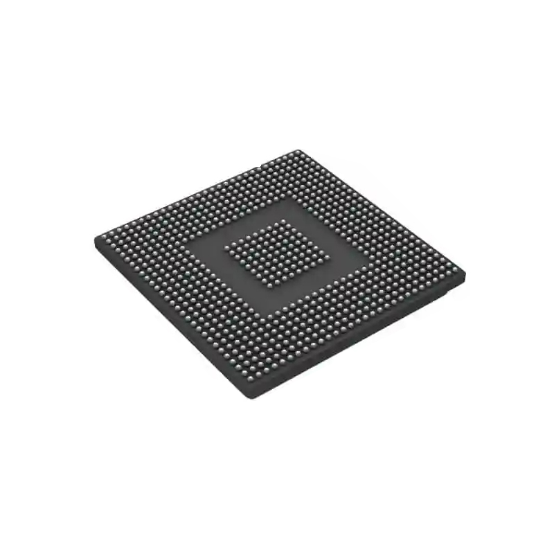
パッケージ/ケース: BGA-484
製品の種類: プログラマブルロジックIC
5CSEBA2U19C8SN 概要
Single ARM® Cortex®-A9 MPCore™ with CoreSight™ System On Chip (SOC) IC Cyclone® V SE FPGA - 25K Logic Elements 600MHz 484-UBGA (19x19)
 Inventory")
仕様
| パラメータ | 価値 | パラメータ | 価値 |
|---|---|---|---|
| feature-family-name | Cyclone® V SE | feature-process-technology | 28nm |
| feature-maximum-number-of-user-i-os | 66 | feature-number-of-registers | 37736 |
| feature-device-logic-cells | 25000 | feature-device-system-gates | |
| feature-number-of-multipliers | 72 (18x19) | feature-program-memory-type | SRAM |
| feature-ram-bits-kbit | 1400 | feature-total-number-of-block-ram | |
| feature-ethernet-macs | 2 | feature-supported-ip-core | |
| feature-supported-ip-core-manufacture | feature-maximum-number-of-serdes-channels | ||
| feature-device-logic-units | 25000 | feature-device-number-of-dlls-plls | 5 |
| feature-transceiver-blocks | feature-transceiver-speed-gbps | ||
| feature-dedicated-dsp | 36 | feature-pci-blocks | |
| feature-programmability | Yes | feature-maximum-internal-frequency-mhz | |
| feature-speed-grade | 8 | feature-giga-multiply-accumulates-per-second | |
| feature-differential-i-o-standards-supported | LVPECL|LVDS | feature-single-ended-i-o-standards-supported | LVTTL|LVCMOS |
| feature-external-memory-interface | DDR2 SDRAM|DDR3 SDRAM|LPDDR2 | feature-minimum-operating-supply-voltage-v | 1.07 |
| feature-maximum-operating-supply-voltage-v | 1.13 | feature-packaging | Tray |
| feature-rohs | feature-rad-hard | ||
| feature-pin-count | 484 | feature-supplier-package | UFBGA |
| feature-standard-package-name1 | BGA | feature-cecc-qualified | No |
| feature-esd-protection | feature-escc-qualified | ||
| feature-military | No | feature-aec-qualified | No |
| feature-aec-qualified-number | feature-auto-motive | No | |
| feature-p-pap | No | feature-eccn-code | EAR99 |
| feature-svhc | No |
配送
| 配送タイプ | 配送料 | リードタイム | |
|---|---|---|---|
 |
DHL | $20.00-$40.00 (0.50 KG) | 2-5 日々 |
 |
フェデックス | $20.00-$40.00 (0.50 KG) | 2-5 日々 |
 |
UPS | $20.00-$40.00 (0.50 KG) | 2-5 日々 |
 |
TNT | $20.00-$40.00 (0.50 KG) | 2-5 日々 |
 |
EMS | $20.00-$40.00 (0.50 KG) | 2-5 日々 |
 |
登録された航空便 | $20.00-$40.00 (0.50 KG) | 2-5 日々 |
処理時間:送料は地域や国によって異なります。
支払い
| 支払条件 | ハンドフィー | |
|---|---|---|
 |
電信送金 | 銀行手数料 US$30.00 を請求します。 |
 |
ペイパル | 4.0%のサービス料がかかります。 |
 |
クレジットカード | 3.5%のサービス料がかかります。 |
 |
ウエスタンユニオン | charge US.00 banking fee. |
 |
送金サービス | 銀行手数料は 0.00 米ドルかかります。 |
保証
1.購入した電子部品には365日保証が含まれており、製品の品質を保証します。
2.受け取った商品の一部が完璧な品質ではない場合、当社は責任を持って返金または交換を手配します。 ただし、商品は元の状態のままでなければなりません。
パッキング
-

ステップ1 :製品
-

ステップ2 :真空包装
-

ステップ3 :静電気防止袋
-

ステップ4 :個包装
-

ステップ5 :梱包箱
-

ステップ6 :バーコード配送タグ


すべての製品は静電気防止袋に梱包されます。 ESD 帯電防止保護を備えた状態で出荷されます。
社外の ESD 梱包ラベルには、部品番号、ブランド、数量などの当社の情報が使用されます。
私たちは出荷前にすべての商品を検査し、すべての製品が良好な状態であることを確認し、部品が新しいオリジナルでデータシートと一致していることを確認します。
すべての商品に問題がないことを確認した後、梱包後、安全に梱包し、グローバルエクスプレスで発送します。 優れた耐穿刺性と耐引裂性を示し、シールの完全性も良好です。


パーツポイント
-
The 5CSEBA2U19C8SN is a high-performance FPGA (Field-Programmable Gate Array) chip from Intel Altera's Cyclone V series. It features 30,620 logic elements, 1,518 Kbits of embedded memory, and 144 DSP blocks, making it suitable for a wide range of applications requiring customizable hardware acceleration and processing capabilities.
-
Equivalent
The equivalent products of the 5CSEBA2U19C8SN chip are 5CSEBA2U19C8N, 5CSEBA2U19C6N, and 5CSEBA2U19A8N. These chips are also part of the Intel Cyclone V series and offer similar features and applications to the 5CSEBA2U19C8SN. -
Features
1. Intel Cyclone V SE FPGA 2. 19,500 Logic Elements 3. 952 KB Embedded Memory 4. 56 18x18 Multipliers 5. 172,800 Total RAM bits 6. 1,152 Maximum user I/Os 7. 8 Fractional Phase-Locked Loops (PLLs) 8. 266 MHz Maximum core speed 9. Integrated hard IP blocks for PCI Express, DDR3, and more. -
Pinout
The 5CSEBA2U19C8SN is a 324-pin FPGA (Field-Programmable Gate Array) device. It has various functions including logic processing, signal processing, and digital communication. This FPGA also features high-speed transceivers and low power consumption for efficient performance in a range of applications. -
Manufacturer
The manufacturer of 5CSEBA2U19C8SN is Intel Corporation, an American multinational corporation and technology company headquartered in California. Intel is a leading manufacturer of semiconductor chips and other computer hardware components. They are known for producing a wide range of products including microprocessors, chipsets, and other integrated circuits for various devices. -
Application Field
Some application areas of 5CSEBA2U19C8SN include industrial automation, communication systems, automotive electronics, medical devices, and consumer electronics. This FPGA can be used in various industries for implementing complex algorithms, signal processing, and control systems due to its high performance and flexibility. -
Package
The 5CSEBA2U19C8SN chip is a Ball Grid Array (BGA) package type with a size of 19mm x 19mm and a form factor of 484-ball.


データシート PDF
私たちは高品質の製品、思いやりのあるサービス、販売後の保証を提供します
-

豊富な商品を取り揃えておりますので、お客様の様々なニーズにお応え致します。
-

最小注文数量は1個からとなります。
-

最低国際配送料は0.00ドルから
-

全商品365日品質保証


推薦する
-
![EPXA10F1020C1]()
-
![5ASTFD5K3F40I3N]()
-
![EPCS64N]()
Altera Corporation (Intel)
-
![EPM7064STC44]()
Altera Corporation (Intel)
-
![EP4CE55F23]()
Altera Corporation (Intel)
-
![EP3C16F484]()
Altera Corporation (Intel)


Quality of the components received was great, couldn't be happier with my purchase.